11Embedded Die in Substrate (Panel‐Level) Packaging Technology
Tomoko Takahashi and Akio Katsumata
J‐Devices
11.1 Technology Description
With square or rectangular panels instead of circular wafers, panel‐level packaging has more die per panel than an equivalent size round wafer with its edge and missing die losses, potentially providing significant cost savings. Similar to other advanced packaging techniques, a fan‐out (FO) technique is required to achieve higher integration levels and a greater number of external connections. The fan‐out panel‐level package (FO‐PLP) described in this chapter is unique, because a metal material was selected as the base plate of an FO package. The base plate was not a temporary structure to place die on, but was a part of the package as shown in Figure 11.1.
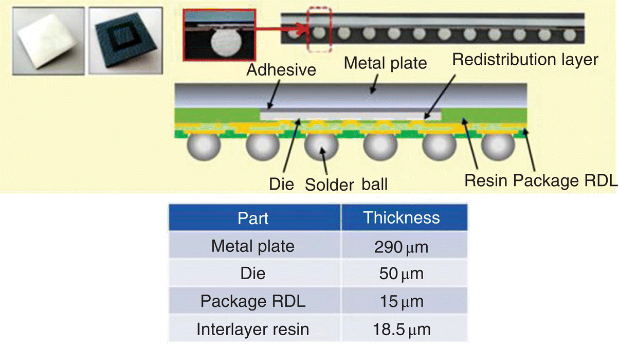
Figure 11.1 Fan‐out package using a metal base plate.
The main technology issue of panel‐level assembly is how to laminate resin, similar to the substrate manufacturing process using laminate dielectric layers, on metal without delamination, warpage, or deformation during processing. To address this issue, J‐Devices adds a stress release layer between the metal and the resin. This layer releases the stress caused by the coefficient of thermal expansion (CTE) mismatch among layers during the assembly process. With this approach, the warpage of the panel is well controlled and can be ...
Get Advances in Embedded and Fan-Out Wafer Level Packaging Technologies now with the O’Reilly learning platform.
O’Reilly members experience books, live events, courses curated by job role, and more from O’Reilly and nearly 200 top publishers.

