Appendix D
Process Parameters and Chips Specifications
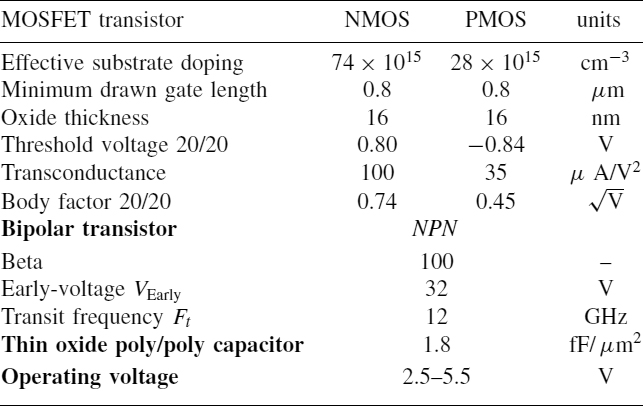
D.1 AMS 0.8 μm BiCMOS Process
The AustriaMicroSystems AMS 0.8 μm BiCMOS process is a mixed analog/digital process and offers the implementation of a generic npn–bipolar transistor. The process provides two metal layers and two layers of low ohmic polysilicon (poly) to form poly/poly capacitors. The substrate is acceptor doped (p−) and the gates consist of heavily donor-doped polysilicon (n+). This process was available through the multi-project-wafer (MPW) service provided by Europractice (www.europractice.com). The most important process parameters are listed in Table D.1.
Table D.1 AMS 0.8 μm BiCMOS process parameters.
D.2 Chip Specifications
Table D.2 Specification of the three visual motion chips presented in this book.
| The smooth optical flow chip | |
| Die size(s) | 2.55 × 2.55 mm2 / 4.72 × 4.5 mm2 |
| Array size(s) (motion units) | 10 × 10/30 × 30 |
| Pixel size | 124 × 124 μm2 |
| Active elements | 119 |
| Power dissipation | 52 μW |
| Outputs (scanned) | optical flow, photoreceptor |
| Typical read-out speed | 1000 frames/s |
| The motion segmentation chip | |
| Die size | 2.7 × 2.95 mm2 |
| Array size (motion units) | 11 × 11 |
| Pixel size | 170 × 170 μm2 |
| Active elements (per pixel) | 203 |
| Fill factora | 2.1% |
| Power dissipation (per pixel) | 80 μW |
| Outputs signals (scanned) | 5: photoreceptor, optical flow, P and Q |
| Max. read-out speed | ≈10, 000 frames/s |
Get Analog VLSI Circuits for the Perception of Visual Motion now with the O’Reilly learning platform.
O’Reilly members experience books, live events, courses curated by job role, and more from O’Reilly and nearly 200 top publishers.

