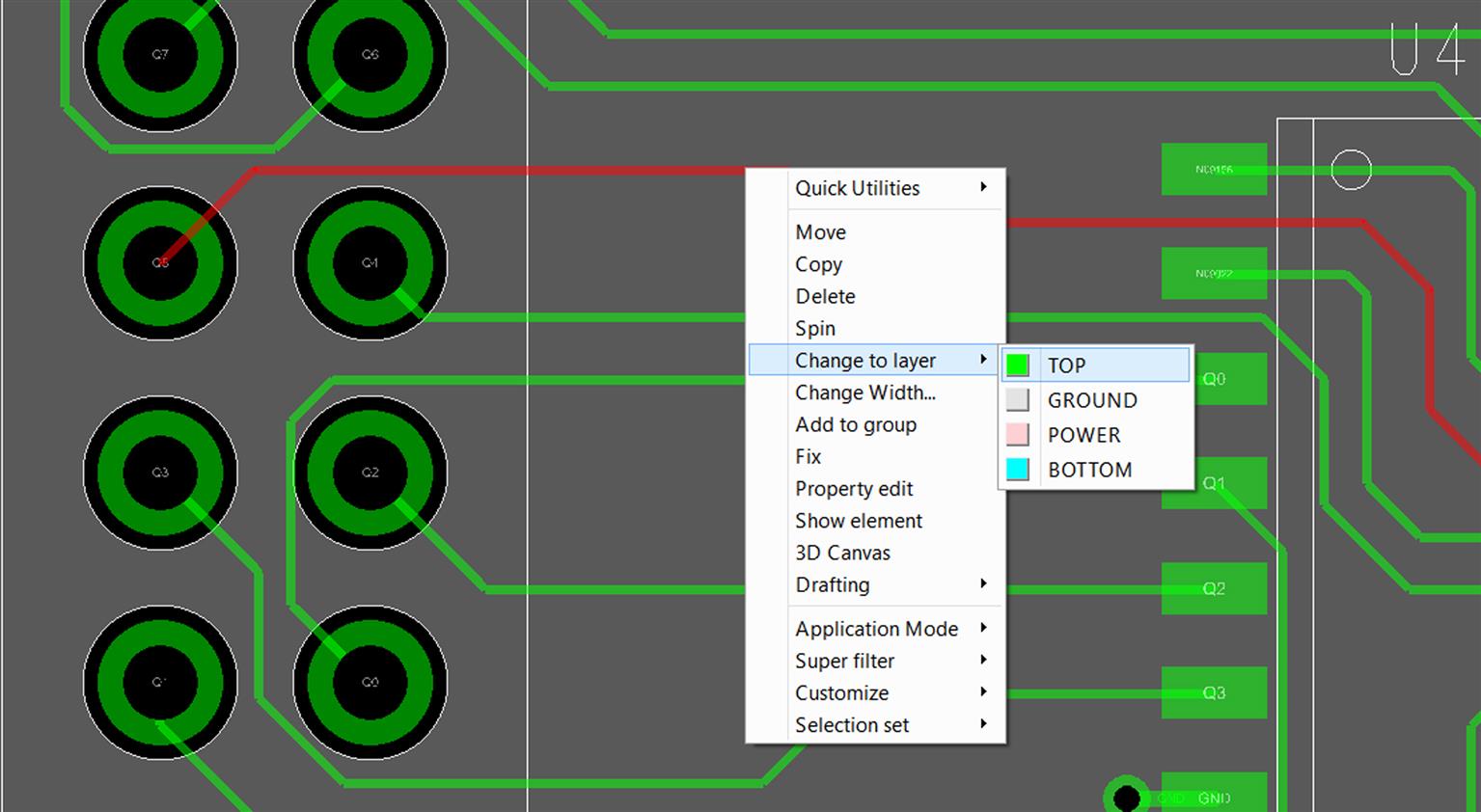
Adding Ground Planes and guard traces to Routing layers
As discussed at the beginning of these examples and in Chapter 6, Printed circuit board design for signal integrity, you can reduce noise levels on signal lines by surrounding traces with copper planes and guard traces. Not everyone agrees with this practice, but it is demonstrated here in the interest of completeness. The following procedures demonstrate how to use the Add Connect tool to add ground nets and use shapes to add copper planes to Routing layers.
Routing guard traces and rings
If you have one or two traces that could have cross-talk ...
Get Complete PCB Design Using OrCAD Capture and PCB Editor, 2nd Edition now with the O’Reilly learning platform.
O’Reilly members experience books, live events, courses curated by job role, and more from O’Reilly and nearly 200 top publishers.

