6.5 Embedded Microstrip
There are several benefits to be gained when outer trace layers are embedded in a dielectric. Traces are not plated when the holes are plated. This allows tighter control of characteristic impedance. The reactive terms contributing to cross talk are more apt to cancel. This reduces the amplitude of the forward cross-coupled wave. The traces are not plated, so sur face currents flow in copper and not in solder. This reduces transmission line losses due to skin effect.
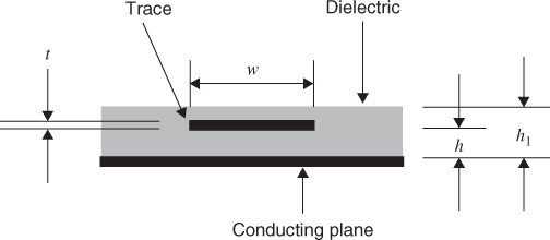
The geometry of embedded microstrip is shown in Figure 6.11.
Figure 6.11 The geometry of embedded microstrip.
The equation for the characteristic impedance of embedded microstrip is
6.3 ![]()
where h1 > 1.2h and ε R < 15. The effective dielectric constant ε ′ is
6.4 ![]()
For 2 mil of dielectric over the trace, the effect is to lower the characteristic impedance by about 1%. Refer to Figures 6.2–6.4 for curves that show how the geometry must change to keep the characteristic impedance constant.
Get Digital Circuit Boards: Mach 1 GHz now with the O’Reilly learning platform.
O’Reilly members experience books, live events, courses curated by job role, and more from O’Reilly and nearly 200 top publishers.

