Atomically Controlled Processing forFuture Si-Based Devices
Laboratory for Nanoelectronics and SpintronicsRIEC, Tohoku University, 2-1-1 Katahira, Aoba-ku, Sendai 980-8577, Japan
IHP, Im Technologiepark 25, 15236 Frankfurt (Oder), Germany
1. Introduction
Atomically controlled processing for group IV semiconductors has become indispensable for the fabrication of ultrasmall MOS devices for ULSI, because high performance devices require atomically abrupt heterointerfaces and doping profiles, as well as strain engineering due to introduction of Ge into Si. In the fabrication of high performance devices, there are many surface reaction processes, typically by chemical vapor deposition (CVD). Further progress in CVD process technology requires atomic-order surface reaction control, as well as low-temperature processing, in order to suppress thermal degradation such as unexpected reactions and impurity diffusion. Improvements in the quality of gases and equipment have enabled ultraclean low-temperature processing for atomic-order control.1-3
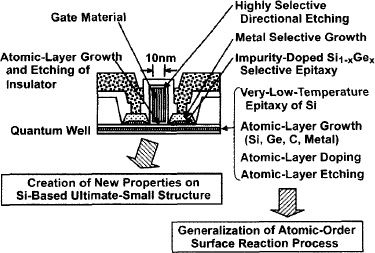
Figure 1. Atomically controlled processing for group IV semiconductors for ultrasmall and nanodevices.
Our concept of atomically controlled processing for group IV semiconductors is based on atomic-order surface reactions. The final goal is the generalization of the atomic-order surface reaction processes ...
Get Future Trends in Microelectronics: Up the Nano Creek now with the O’Reilly learning platform.
O’Reilly members experience books, live events, courses curated by job role, and more from O’Reilly and nearly 200 top publishers.

