6.1. Silicon Epitaxy—The Basics
Epitaxy was invented at AT&T Bell Labs [2] circa 1960 in order to improve doping profile abruptness and increase the operating frequencies of bipolar transistors. Since then, the use of epitaxy has spread throughout the semiconductor industry and can be found in nearly all fabrication disciplines. Although the details of epitaxial deposition recipes are often highly specific to the precise goals of the process, with respect to MEMS applications, the process can often be represented by Figure 6.1.
Fig 6.1. The basic epitaxy process recipe.
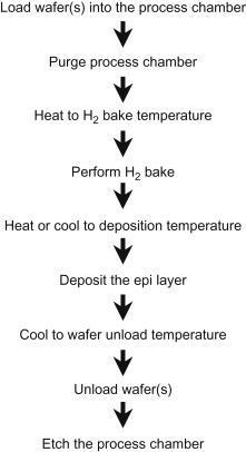
Silicon substrates (wafers) are loaded into the process chamber and the ...
Get Handbook of Silicon Based MEMS Materials and Technologies now with the O’Reilly learning platform.
O’Reilly members experience books, live events, courses curated by job role, and more from O’Reilly and nearly 200 top publishers.

