9.3 Voltage and Current Common Mode Component
As mentioned at the beginning of this chapter, unwanted bearing currents appear in the drives with voltage inverters. This occurs because the voltage inverter with classical pulse width modulation (PWM) is a source of CM voltage, which forces the bearing current to flow.
To clarify the CM voltage effect, the voltage inverter structure presented in Figure 9.3 is analyzed.
Figure 9.3 Structure of the voltage inverter with output voltages notations
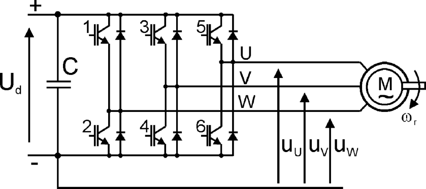
In voltage inverters, only one of eight transistor switching combinations is possible. Due to the voltage notation presented in Figure 9.3, the inverter output voltages for each of the eight states are presented in Table 9.1.
Table 9.1 Voltage inverter output voltages for possible switching combination.
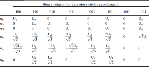
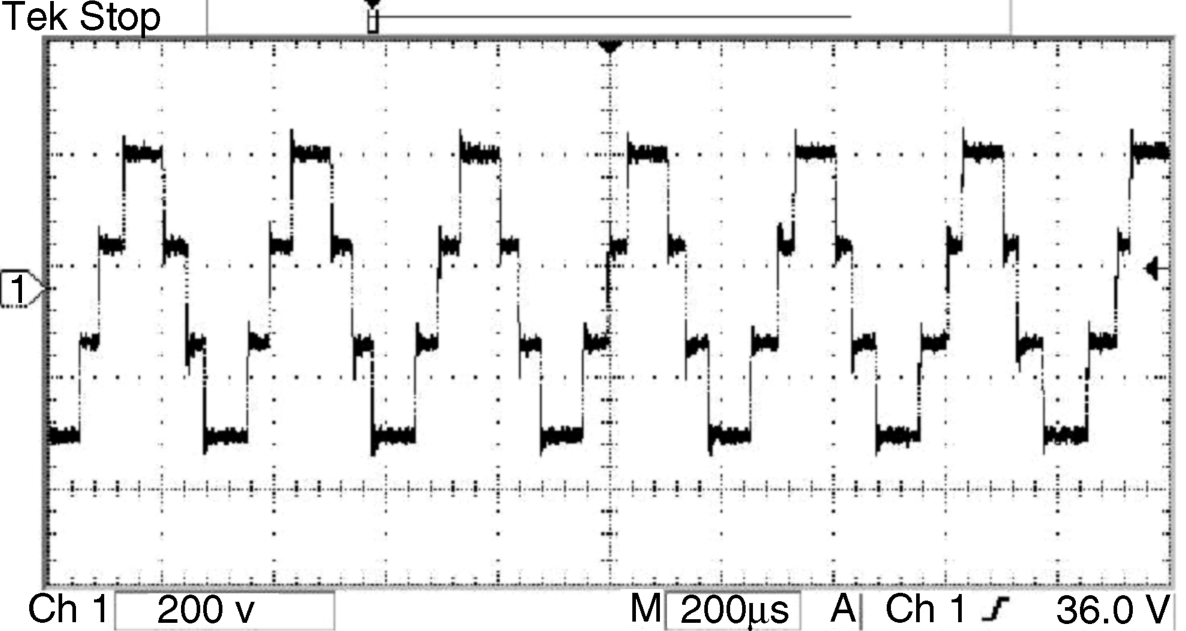
It is noted that the zero-component voltage changes according to changes in the transistors switching combination. The peak value of the u0 voltage is very high and equal to the inverter DC link voltage Ud. The u0 frequency is equal to the inverter PWM switching frequency. A typical u0 voltage waveform is presented in Figure 9.4.
Figure 9.4 The CM voltage waveform in a voltage inverter
9.3.1 MATLAB/Simulink ...
Get High Performance Control of AC Drives with Matlab / Simulink Models now with the O’Reilly learning platform.
O’Reilly members experience books, live events, courses curated by job role, and more from O’Reilly and nearly 200 top publishers.

