Receive Logic Details
Figure 11-20 shows the receiver logic of the Logical Physical Layer. This section describes packet processing from the time the data is received serially on each Lane until the packet byte stream is clocked to the Data Link Layer.
Figure 11-20. Physical Layer Receive Logic Details
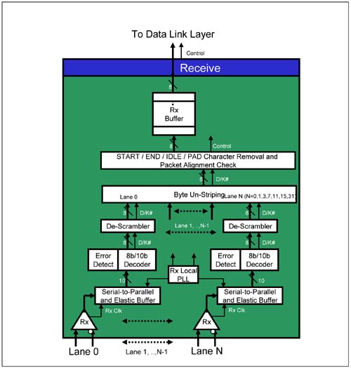
Figure 11-21 illustrates the receiver logic's front end on each Lane. This is comprised of:
The differential receiver.
The Rx Clock recovery logic.
The COM symbol and Ordered-Set detector.
The Serial-to-Parallel converter (Deserializer).
The Lane-to-Lane De-Skew logic (delay circuit).
The Elastic Buffer and Clock Tolerance Compensation logic.
Figure ...
Get PCI Express System Architecture now with the O’Reilly learning platform.
O’Reilly members experience books, live events, courses curated by job role, and more from O’Reilly and nearly 200 top publishers.

