13.9 PROBLEMS
- (a) Verify that the circuit in Fig. 13.39 implements a binary full-adder.
(b) The adder circuit in Fig. 13.39 uses 32 transistors. Derive an optimized architecture using CMOS-transmission gates with only 24 transistors (Hint: Try to share hardware of sum and carry parts).
(c) What is the number of transistors in the critical path of an 8-bit carry-ripple adder?
- Consider the addition of 2 two’s complement 8-bit numbers X and Y in a ripple-carry manner as shown in Fig. 13.40.
Derive a truth table and logic circuit for detecting overflow for this adder using the bits x7, y7, c7, c8, and s7. (Hint: If x7 ≠ y7, i.e., the sign bits of X and Y are different, then there can never be overflow. If x7 = y7, then overflow occurs if x7 = y7 ≠ s7.)
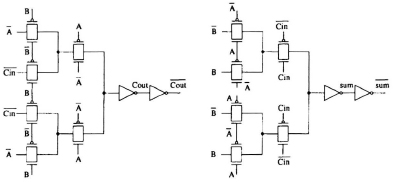
Fig. 13.39 Schematic of a complementary pass-transistor logic based CMOS full-adder.
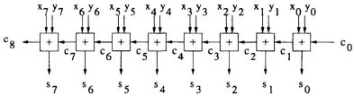
Fig. 13.40 Eight-bit ripple carry adder in Problem 2.
- Design bit-parallel architectures for computation of
using
(a) carry-save arithmetic and
(b) tree-height reduction technique,
using half and full adders and a VMA. Assume a wordlength of 8. Compute the latencies of these architectures without including the latency of the VMA.
- This problem ...
Get VLSI Digital Signal Processing Systems: Design and Implementation now with the O’Reilly learning platform.
O’Reilly members experience books, live events, courses curated by job role, and more from O’Reilly and nearly 200 top publishers.

