Chapter 8
Optics and Optronics
“Optics rule: everything seen from a distance look larger”
Extract from Nouvelles pensées échevelées,
Stanislaw Jerzy Lec (1909–1966)
8.1. Overview
We discuss the “physical layer” of wireless optical terminals in this chapter. The digital communication part and the communication protocol part will be discussed in Chapter 10 (OSI layers 1 and 2 and the TCP/IP layer 1).
The other layers are application oriented and will not be considered in this book.
The different modules of a wireless optical terminal are illustrated in Figures 8.1 and 8.2.
8.2. Optronics: transmitters and receivers
8.2.1. Overviews on materials and structures
The transmitter and receiver components of this section are components of very small dimensions (volumes below 1 mm3) processed by deposition of thin films on semiconductor materials.
A crystal of semiconductor material is a poor conductor. The electrons which are the charge carriers are not free to move within the material when they occupy energy states in the low-energy valence band. They can only contribute to the current flow when they get enough energy in excess of the bandgap and are free in the conduction band as shown in Figure 8.3.
Figure 8.1. Diagram of an optical wireless transmitter
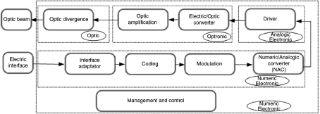
Figure 8.2. Diagram of an optical wireless receiver
This excess in energy needed to gain kinetic energy and be admitted into ...
Get Wireless Optical Telecommunications now with the O’Reilly learning platform.
O’Reilly members experience books, live events, courses curated by job role, and more from O’Reilly and nearly 200 top publishers.

