Chapter 4. Power Systems
Providing system power can be a simple matter, but for complex systems it can turn into a significant design issue. Power and ground (P&G) are common to an entire system and can be a smoky failure point, a common path for noise into the entire system, or a path where the power demand in one place affects the performance someplace else.
Safe AC power, safe failure scenarios, regulatory compliance issues, suitable noise levels on power, controlled up/down power cycles, and stable power under highly variable loads are all part of a reliable system. Understanding the options available among power converters and how to configure the power system is the goal. Designing an AC/DC converter from scratch is rarely necessary, as many off-the-shelf converters are available that are easily implemented into a system.
After initial AC/DC power conversion, additional items such as local regulation, multiple voltages for different circuits, high-frequency bypassing, selective device decoupling, power monitors, and power cycling controls are commonly needed. In addition, several source-power scenarios exist: disposable battery, battery with charging capability, external AC/DC converter, or AC/DC converter inside the system.
This chapter discusses all of these and highlights their similarities and differences.
Split Phase AC Mains Power
What does AC mains power consist of? In the United States at the residential level (Figure 4-1), the AC power grid feeds a local step-down and distribution transformer that creates a “split phase 120/240 system” output.
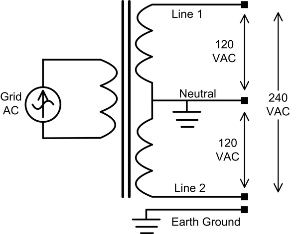
Figure 4-1. AC split phase power, step-down from commercial power grid
Figure 4-2 shows both line signals from the secondary of the step-down transformer. What reaches a typical wall outlet (120 VAC 60 Hz in the United States, and 50 Hz elsewhere) is a three-wire system comprising one line signal (aka hot), neutral, and earth ground. Neutral is the center tap from the secondary in the AC mains step-down transformer.

Figure 4-2. AC split phase power signals
Neutral and ground are only connected back at the AC mains distribution transformer. Prior to 1960, residential wiring was two wires only, without the ground safety, which produced unsafe devices in many failure scenarios.
AC Power Safety: Defining the Problem
When bringing AC power directly into a device, the implementation needs to be carefully considered in the design. Getting things wrong with AC power can lead to deadly devices and smoke-filled outcomes.
Most devices now use low-voltage DC power internally, provided from an external AC/DC converter, thus allowing most designers to remain blissfully unaware of high-voltage product safety requirements. Many older (prior to 1960) electrical products were inherently unsafe or could become deadly with a single fault failure. Metal enclosures were commonly used (prior to the widespread use of plastics), and lack of a ground safety connection made for a deadly combination. Thankfully, most electrical devices prior to 1960 have been retired or superseded by newer product offerings, so most of those devices are no longer in use.
High-Voltage and Low-Voltage Partitioning
Designing with power inlets lower than 50 V is classified as extra low voltage (ELV), and that simplifies things. Safety issue requirements are primarily placed on anything classified as high voltage (HV), namely the AC/DC converter.
Figure 4-3 shows one method that is commonly used, where both the AC/DC converter and the electronic system are enclosed in a conductive metal enclosure and a safety ground is tied back to the AC mains safety ground. This widely used approach is commonly employed in many desktop personal computers.
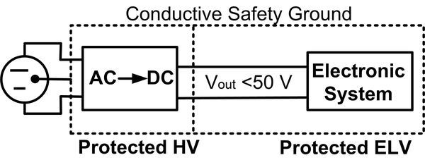
Figure 4-3. Protected HV with protected ELV DC
ELV devices are subdivided into separated ELV (no ground return path is used) and protected ELV (a ground earth safety is attached). The safety standard IEC 62368-1 (Safety Requirements for Audio/Video, Information & Communication Technology Equipment) has become the most commonly used standard for ELV safety.
Figure 4-4 shows an alternative method, where the enclosure is an insulator and is not grounded. To meet safety requirements on the HV portion, a double insulated technique is used. Double insulated devices utilize two layers of protective insulation, so if one layer fails, the device remains safe to handle.

Figure 4-4. Double insulated HV with separated ELV DC
For ELV devices, safety requirements are minimal, with some form of overcurrent protection and a nonconductive enclosure generally being sufficient.
In Figure 4-5, an AC/DC power supply is in a double insulated structure and has an ELV power cord output. Many commercially available versions of this exist, with full regulatory testing already done. Using this type of AC/DC power supply, designers can create their electronic system as a separate entity that requires the least possible ELV testing. This approach is ubiquitous and is utilized in a myriad of consumer electronics devices.

Figure 4-5. Standalone double insulated HV powering a separated ELV device
Safe Failure Methods and Single Fault Safe Scenarios
Normal operational safety is the start, but when something breaks, power systems also require a safe failure method. The single fault safe concept is simple: any element of the system can fail in an open circuit state or closed circuit state, or can contact any other element in the system and not cause danger to the user.
Introduction of a ground safety return path into modern power wiring allowed for a safe system in most single fault situations, where the grounded enclosure, in conjunction with a fused line connection, could keep a device safe.
The principal regulatory safety standards for power systems are:
IEC 61140: Protection Against Electric Shock Common Aspects for Installation and Equipment
IEC 62368-1: Audio/Video, Information and Communication Technology Equipment, Part 1 Safety Requirements
These standards are referenced in this chapter. Designers should acquire the latest versions.
According to IEC 61140, devices that use a metal chassis and enclosure structure that is attached to a ground safety connection are defined as Class I devices. Their failure safety is dependent upon the presence of a properly connected external ground. Some devices have only line and neutral connections, and they meet safety requirements using a double insulated structure. For these devices, the internal wiring and circuits are within a secondary insulating enclosure. In this manner, the device can have a single fault failure without exposing users to high-voltage contact.
Double insulated devices are considered Class II devices and the safety redundancy of the device is not dependent on an external ground. Consequently, double insulated devices are popular in electric power tools, due to remaining safe when connected to electrical power with questionable ground paths, as frequently happens in construction environments.
ELV systems are Class III devices under the IEC 61140 regulatory standard.
If the AC/DC converter is placed inside the product, the whole product needs to meet Class I or Class II safety requirements of a grounded enclosure or double insulated configuration. Using an AC/DC converter externally circumvents that restriction and is a popular approach to the problem.
Overcurrent Protection Methods and the Weakest Link
Overcurrent protection is the most basic form of system protection. There are four common ways to turn things off in an overcurrent situation:
Fuses
Circuit breakers
Polymeric positive temperature coefficient (PTC or PPTC) resettable fuses
Active circuit methods
Fuses are commonly used for their simplicity and low cost. However, fuses can be too slow, they require manual replacement to restart the system, and they are not terribly accurate. In some situations, it is desirable to control both the current and the time needed for the fuse to do its job. However, the overcurrent amount and the activation time are interactive, so don’t expect fast and accurate from a fuse.
Nonetheless, the fuse is often fast and accurate enough. That, combined with low cost, simplicity, and reliability, makes fuses the go-to solution in many cases. If the fuse is expected to blow only when something major on the printed circuit board (PCB) fails, a soldered-in surface mount fuse can be used with minimal cost and excellent reliability. Fuses don’t need to be replaced in many cases, and socket mounting is unnecessary.
Circuit breakers suffer many of the limitations of fuses, with speed and accuracy being “good enough” for most situations. To gain the convenience of a resettable device, the penalty is paid in cost and size.
A circuit breaker is considerably more expensive than a fuse. Also, circuit breaker reliability can suffer in hostile environments due to internal corrosion issues if they are not hermetically sealed. Generally, circuit breakers are called for when the designer expects frequent overcurrent situations due to the application.
Polymeric positive temperature coefficient devices (widely known as PTC or PPTC devices) can be considered self-resetting fuses. They warm up, due to overload current, and go into a high-resistance mode, limiting the current until they cool off, and then return to a low-resistance state.
PTC devices do have some less-than-ideal internal on/off resistance, but they serve well in situations where auto-reset is desirable. The PTC has limitations of accuracy and response time, as all thermally triggered devices do. Nonetheless, generally the PTC can be included on a PCB for a low-cost design solution.
Active circuit protection for overcurrent detection and shutdown comes in many variants. The basic concept is a set of detection circuits for current and/or voltage to determine whether the applied power is outside specified limits, which triggers suitable circuit controls to shut down or limit performance.
Active circuit systems can be fast and accurate if needed. The price paid here is in complexity and cost. Frequently, this approach is unneeded and one of the simpler methods is suitable.
Many switching AC/DC converters use active circuit methods within their design to protect circuits that can self-destruct more quickly than a fuse can respond. Seek out this feature when selecting AC/DC converters. Look for information that indicates the device is “self-protecting” or “overcurrent protected” or “current limited” in the specification.
Regardless of overcurrent protection method, the system needs to make sure the “weakest link” is the actual protection device. If the PCB traces melt at 1 A of current and the protection device opens at 2 A, something wasn’t designed properly. Also, the parameters for the trip protection point need to consider both min/max sustained and startup surge currents. As a simple guideline, setting a fuse value at twice the maximum current seen in normal circuit operation is often suitable.
Systems may have high-current and low-current sections where a failure in the low-current section requires a lower value protection shutdown for that part of the system. A common design mistake is to use a single overcurrent shutdown in a situation where a low-power part of the system self-destructs since it is powered in parallel with the high-current part of the system.
Thermal monitoring of high-power devices can be useful, with protection control built into the system. For some devices, this provides another layer of safety and capability to stress devices close to their thermal limits without self-destruction. Older devices used thermocouples, or thermistors, but silicon-based thermal monitors with digital interfaces to a local controller are a more modern approach. Most modern high-performance microprocessors use thermal sensors within the IC (FDI: Sense).
AC/DC Conversion
Very few electronic devices use AC power directly. The majority of devices use DC power, and most modern electronics use 5 V and lower power sources.
Systems with DC motors or other high-power devices may need higher voltages. Due to this, the first converter in the system will be an AC/DC converter, with sufficient voltage to support the high-voltage devices.
The Classic Approach: 60 Hz Transformers
As shown in Figure 4-6, the classic approach to AC/DC conversion uses a transformer at 60 Hz (or 50 Hz, depending on the country). This seems simple: step down the AC voltage, put the reduced AC voltage through a diode bridge, and filter the rectified AC for a DC output.
While the idea is simple, certain pieces tend to be both big and expensive. The problem here is the low frequency of AC mains power. A 60 Hz transformer will be both bulky and heavy. For the same power rating, the transformer size decreases as the frequency increases. In addition, the output filter capacitor has to accurately maintain the output voltage under high-current loads between the rectified peaks of the 60 Hz waveform. This necessitates the use of a large electrolytic filter capacitor. By increasing the frequency, the size of both the transformer and the filter capacitor can be decreased. The aviation industry often uses 400 Hz AC power to take advantage of this.

Figure 4-6. Classic 60 Hz AC-to-DC converter with iron core transformer
There are better methods than putting 60 Hz AC into a transformer.
Off-line Switchers
The limitations of the 60 Hz AC-to-DC converter are circumvented with a switched mode conversion method commonly known as an off-line switcher (Figure 4-7). This approach rectifies the AC line voltage, and uses C1 to maintain a high DC voltage where ripple and accuracy are not critical. That DC voltage is rapidly pulsed across the primary of T1 with a switch. The switching frequency is much higher than 60 Hz, with 10 KHz to 1 MHz commonly used.
Although appearing more complex, off-line switchers offer several advantages. Using a higher frequency allows for a much smaller transformer (T1) and output filter capacitor (C2). The high-voltage DC at C1 can vary widely, so C1 does not need to be very large.
This method is used in virtually all AC/DC converters today, with small form factor implementations illustrated by the numerous USB and cell phone chargers that sit readily within an AC power plug footprint.
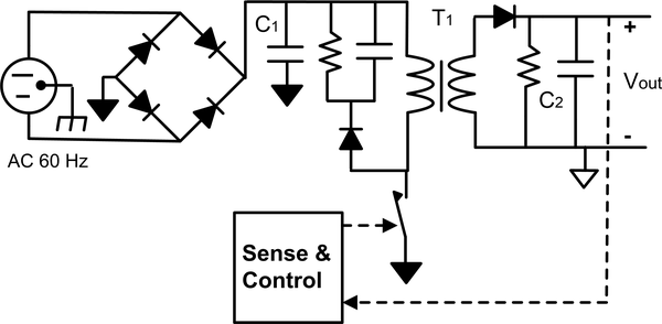
Figure 4-7. AC/DC converter with off-line switcher
A broad selection of off-line switching AC/DC converters are available for off-the-shelf purchase. The 60 Hz transformer method is much larger and more costly to implement. Due to this, the 60 Hz step-down transformer is largely obsolete in consumer electronics.
The AC/DC converter generally provides a single DC voltage and is commonly selected to be the highest DC voltage that the system needs. Other power regulators, for DC/DC conversion, are then used to complete the system power requirements.
Multi-PCB Systems: The Need for Local Power Regulation
In Figure 4-8, the impedance of power and ground wires, combined with dynamic current loads, will create both ground bounce and power sag on various circuit boards. A design can reduce this effect with shorter (less inductance) and thicker (lower resistance) wires, but will not eliminate it. Consequently, a multi-PCB design must deal with both ground and power voltage variance between PCBs.
Separate regulators on each PCB to create locally needed voltages is the widely used solution (Figure 4-8). Systems with multiple circuit boards can use a common AC/DC converter to distribute a “raw” DC voltage. This DC voltage should have “headroom,” namely several volts larger than the minimum required by each of the satellite PCBs. With the added voltage headroom, the effects of ground bounce between PCBs and voltage sag can then be removed by the local voltage regulator, and each PCB will be able to tolerate P&G variance at the power input.
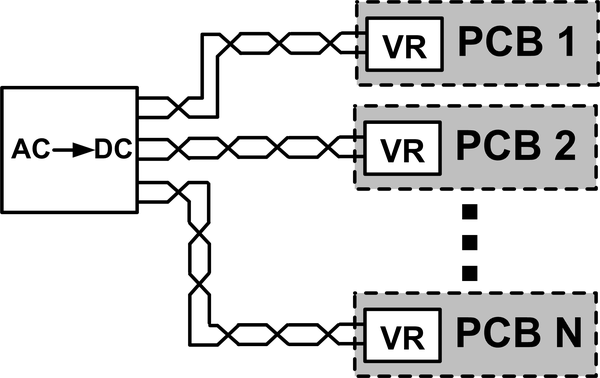
Figure 4-8. Multi-PCB systems with local voltage regulation
Many industrial systems distribute raw DC power at 36 V, 24 V, or 12 V depending on what the satellite PCBs require. Directly using a DC voltage created off the PCB without a local regulator will never be consistent or noiseless, and frequently causes failures during electromagnetic compatibility (EMC) regulatory testing. Therefore, one should regulate the power supply locally on the same PCB where it is used.
DC/DC Conversion: Linear Versus Switching
Power regulators can be divided into two groups, linear regulators and switching regulators, which use distinctly different methods to provide a consistent voltage output. Linear regulators include emitter follower regulators and low-dropout (LDO) regulators. Switching regulators include buck converters, which reduce voltage; boost converters, which increase voltage; and buck-boost converters, which can reduce or increase voltage output. Other switched-mode power supply (SMPS) configurations exist, but these are the ones most commonly used.
Linear Regulators: Conceptual
Conceptually, a linear regulator (Figure 4-9) uses adaptive voltage division. As Rload changes, a sense/control circuit adjusts the regulator to maintain Vout.
In Figure 4-9, a power transistor is serving as a variable resistor. The important thing to recognize is that this method creates an output voltage by burning energy inside the regulator. Therefore, don’t expect efficient energy use when implementing a linear regulator. Also, power dissipated (Pburned) by the device can be quite high depending on the current (Iout) and the voltage drop (Vin – Vout) across the regulator. The power dissipated needs to be carefully considered so that the regulator does not thermally fail.
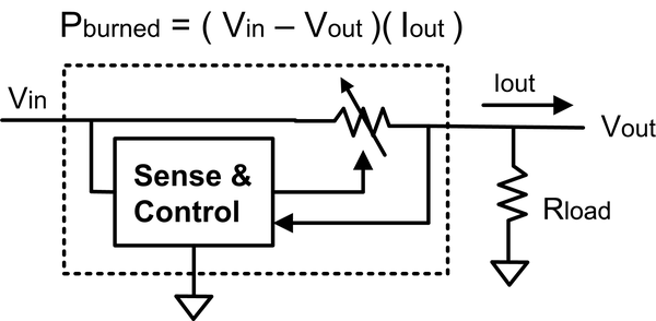
Figure 4-9. Conceptual linear regulator
The primary advantages of linear regulators are that they are electrically quiet in both radiated emissions, and they create a fairly quiet output voltage. The big disadvantages are that they are energy inefficient and often not viable for large input-to-output voltage drops.
Emitter Follower Regulators Versus LDO
Figure 4-10 shows the oldest version of the linear regulator, the emitter follower configuration. A sense and control circuit applies an appropriate control voltage to the base-emitter junction of a transistor to produce the output voltage. The transistor serves as the top half of the voltage divider and is commonly implemented with an NPN bipolar device. When the control voltage goes up, the output voltage follows along. Due to the internal circuit design, the input voltage typically needs to be 2 V greater than the output voltage to function properly.
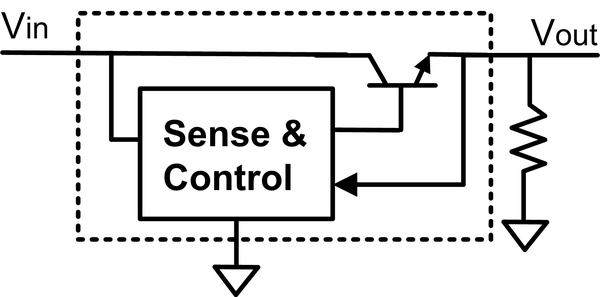
Figure 4-10. Linear voltage regulator, emitter follower
The emitter follower regulator configuration is widely used in the 7800 series (7805, 7812, etc., from multiple vendors) of voltage regulators that have been available since 1970.
Figure 4-11 shows a more modern variant of the linear regulator, the LDO regulator. The LDO regulator uses a power transistor that requires the control voltage presented to the power transistor to go down to increase the output voltage. This is done with either a PNP bipolar transistor or a PMOS MOSFET. By doing this, the necessary input voltage to maintain a proper output is greatly reduced.
LDO devices typically will work down to an input voltage that is 100 mV greater than the output. Due to that capability, the LDO is widely accepted as a more versatile linear regulator than the emitter follower configuration. The LDO still has the limitations of being an active voltage divider method and the associated inefficient use of power, however.
LDO regulators can also exhibit some feedback stability issues if not properly loaded and compensated as per vendor’s recommendations for their specific devices. Carefully read the application documentation to avoid problems.
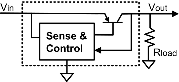
Figure 4-11. Linear voltage regulator, low dropout
Switching Step-Down (Buck) Converter
The switching step-down converter, commonly called a buck converter, uses varying duty cycle methods to reduce an input voltage (Figure 4-12). The switch is turned on and off at a high frequency (10 KHz to 1 MHz is common) while a control feedback system determines the time period during which the switch remains on.
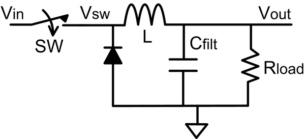
Figure 4-12. Switching step-down converter, conceptual
A higher percentage of on time yields a higher output voltage (Figure 4-13).
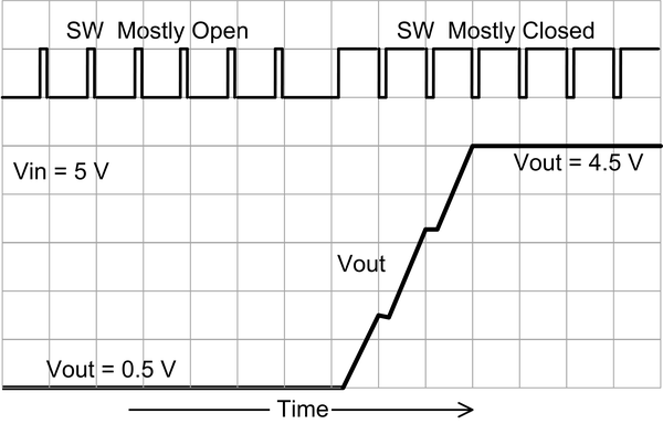
Figure 4-13. Switching constant frequency variable duty cycle
When turned on to a near 100% duty cycle, the output voltage will be close to the input voltage. A reduction in duty cycle will provide proportionally lower voltages at the output. Energy storage for a steady output voltage is maintained on the capacitor, which is fed through the inductor by either the Vin (switch closed) or the magnetic field collapse of the inductor (switch open).
The diode serves as a passive switch, limiting the input side of the inductor to not transition below ground when the switch is open. Higher switching frequencies allow smaller-value inductors and capacitors, thus providing small-size and low-cost implementations. The energy efficiency of the buck converter is very high, typically over 90%, with some losses due to nonideal component characteristics.
Although the overall output voltage remains constant under load, close inspection of the output voltage (Figure 4-14) shows that the switching creates some variance in the output. All switching regulators exhibit this behavior; a variant of a few mV is common in steady state situations. The noise amplitude is dependent on the switching frequency, output current load, inductor value, and capacitor value. Because of this switching noise, the use of switching regulators might not be appropriate in some noise-sensitive situations.
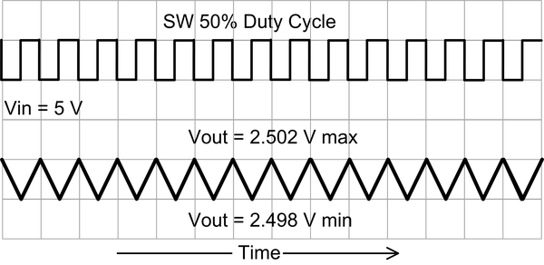
Figure 4-14. Switching converter noise on output
However, this power supply noise is still suitably low to provide acceptable power quality for most applications. Switching regulators are a high-efficiency and versatile solution for all digital power situations, and they can be used for some analog circuits. As such, the use of switching regulators to power analog circuits needs to be carefully considered on a case-by-case basis.
A typical implementation is shown in Figure 4-15, with R1 and R2 allowing a selectable output voltage via feedback (FB) sensing and the capability to enable (EN) the device by an external digital controller.
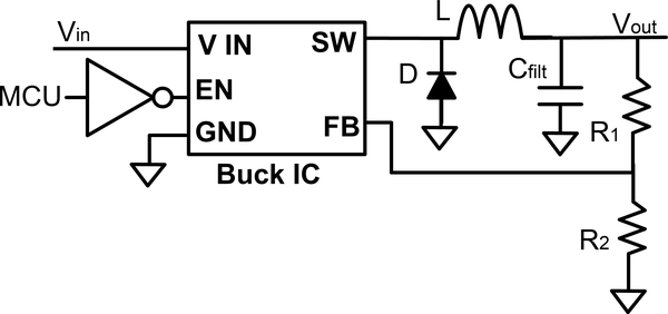
Figure 4-15. Switching step-down (buck) converter implemented
Implementations of the buck converter may include variation in switching frequency, the diode may be internal to the IC, high-power versions may use an external power transistor switch, an active switch can be used in place of the diode for better efficiency, and the feedback sense resistors may be internal to the IC for fixed-voltage versions.
Switching Step-Up (Boost) Converter
The switching step-up converter, known as a boost converter, uses the reactive characteristics of an inductor to create a voltage above the input voltage (Figure 4-16). Closing the switch causes the current to ramp up in the inductor. Opening the switch causes the V = L di/dt to create a positive inductor voltage at the Vsw node, which is in series with the Vin voltage. This forward-biases the diode, dumping charge into the Cfilt and resulting in a Vout above the input voltage Vin.
The switch is turned on and off at a high frequency (10 KHz to 1 MHz is common) while a control feedback system determines the switch’s duty cycle. A higher percentage of the open switch dumps more current into Cfilt, resulting in a higher output voltage.
Energy storage for a steady output voltage is maintained on the capacitor, which is fed through the diode when the switch is open. The diode also serves as a passive switch when the switch is closed, isolating the Cfilt while the magnetic field in the inductor is replenished.
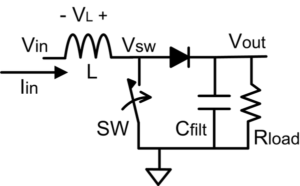
Figure 4-16. Switching step-up (boost) converter, conceptual
Similar to the buck converter, the use of high switching frequencies allows the use of smaller-value inductors and capacitors, enabling small-size and low-cost implementations. A typical implementation is shown in Figure 4-17, with R1 and R2 allowing a selectable output voltage via feedback (FB) sensing and the capability to enable (EN) the device by an external digital controller.
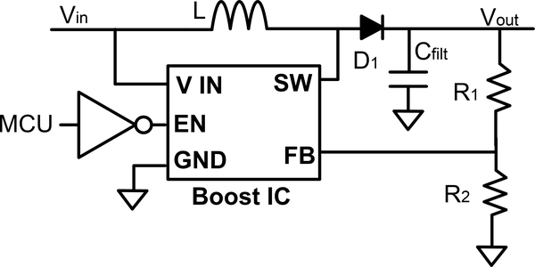
Figure 4-17. Switching step-up (boost) converter, implemented
Variations on the boost converter may include changes to switching frequency, the diode may be internal to the IC, high-power versions may use an external power transistor switch, an active switch can be used in place of the diode for better efficiency, and the feedback sense resistors may be internal to the IC in fixed-voltage variants.
Switching Buck-Boost Converter
A buck-boost converter can either raise or lower the output voltage. Referring to Figure 4-18, when SW1 is actively controlled and SW2 is left open, the device functions as a buck converter. With SW1 closed and SW2 actively controlled, the device functions as a boost converter.
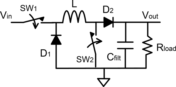
Figure 4-18. Switching buck-boost converter, conceptual
In a typical application (Figure 4-19), the internal control circuitry determines which mode is needed based upon the input voltage available and the target output voltage.
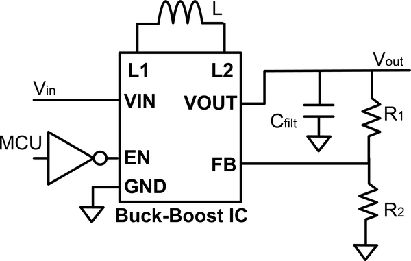
Figure 4-19. Switching buck-boost converter, implemented
The combined buck-boost converter is a useful tool when a widely variable input power supply is used, such as a battery. In these applications, the converter reduces the battery voltage to the target output voltage until the battery has discharged enough to drop below the output target, and then changes mode to a boost converter to extend the useful battery range.
Picking Regulators and Configuring a Power System
Putting a power system together is best illustrated with some examples. Figure 4-20 is the first example and has a 12 V motor driver system, a block of logic that functions from 2.5 V, a host microcontroller (MCU) that needs 3.3 V, and some analog circuitry that needs 5 V. This is a plug-in device that uses an AC/DC converter.
Configuring the power here is mostly straightforward. A 12 V output off-line switcher does the AC/DC conversion and will be used to directly power the motor driver. Motors can be high current, but a limited amount of voltage dip is tolerable during high-current starts.
Motors are also immune to most power noise, and some power variance can be compensated for by the motor controller. The current rating of the AC/DC converter needs to support the start surge current of the motor, the steady state motor current under maximum load, and the other electronics.
When selecting an AC/DC converter, in addition to voltage and current specifications, look for devices that are self-protective and current limiting, and consider the output ripple and noise specifications carefully as the application may have special requirements. If the product will go to markets outside the United States, consider devices that will function off of both 50/60 Hz and 110/220 VAC without the need to change settings or connections.
The 2.5 V logic (Figure 4-20) can be readily provided from a buck converter. The MCU needs 3.3 V and can also use a buck converter. Power for the MCU is always on, and as the central control of the system, it controls all the other power supplies. This allows selective shutdown of peripheral devices and an organized power up/down sequence that provides predictable and safe system behavior.
The analog block that needs 5 V power is not straightforward. More needs to be known, namely how much current is needed and how critical low-noise power is to the circuit. If the circuit can tolerate the power noise associated with a switching supply, it’s the most energy-efficient method. But considering this is a plug-in-the-wall application, energy efficiency is not a high priority.
Using a linear regulator here gives a quiet supply but would be energy inefficient. However, the 5 V output regulator has 12 V input, and that means a 7 V drop across a linear regulator that will be dissipated as heat. In this case, if the current rises to 140 mA, the power burned in the linear regulator rises to 1 W. If the current is low and low-noise power is important, a linear regulator would work.
Check power dissipation in any linear regulator carefully. In many cases, the switching regulator with some filtering may be a viable alternative.
Finally, the system uses fuse protection of 5 A on the motor circuit, which draws a worst-case current of 3 A, and a 0.5 A fuse on the electronics power. Using two fuses is due to the high-current motor circuitry. If a single fuse were used, upon failure the low-current electronics would have to exceed 5 A and that would probably be beyond the destructive current level of the electronics. The 0.5 A fuse mitigates that.
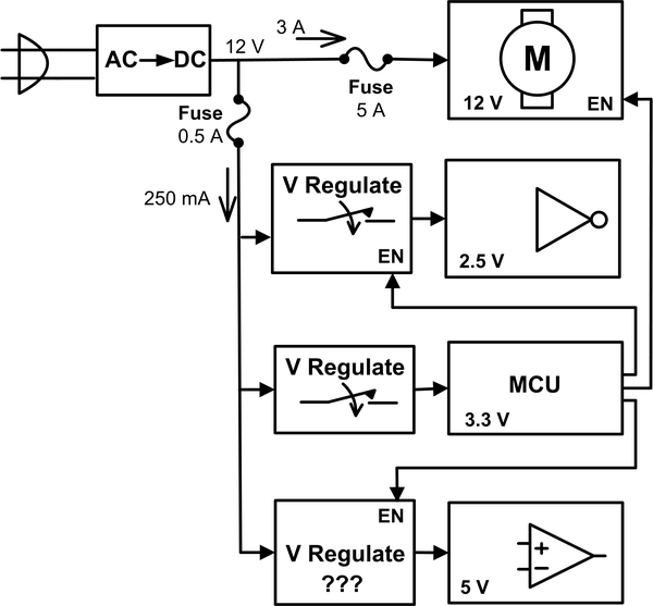
Figure 4-20. Multiple power supplies plug-in device example
Other possible options here include a PTC on the electronics for protection, and a circuit breaker on the motor circuit if the motor application is in a mechanical environment that stalls or goes into overload frequently.
Looking at the second example, shown in Figure 4-21, the power system includes a battery and charger system. This example uses a Lithium battery pack with four batteries in series and two in parallel (eight cells total, 4S-2P). When the charger is applied, the power system sees 18 V, and when the batteries are largely discharged, the power system sees 10 V (FDI: Battery).
Everything needs to function at both voltage extremes. One circuit needs 12 V, which requires a buck-boost converter that functions in buck mode until the battery pack goes below 12 V and then changes to boost mode. Examine the 12 V circuit for noise requirements, which may indicate a need for a filter at the converter output. The digital block that uses 0.9 V power is readily powered from a buck converter.
The MCU runs off 3.3 V and is always powered up from the battery system while controlling the power supplies to the rest of the system. The final block runs off 2.5 V and requires low-noise power input. This device is a good candidate for a linear regulator, using an LDO that is powered off of 3.3 V. The 0.8 V of headroom is sufficient for an LDO device to function without a large voltage drop and the associated power lost as heat.
Carefully examine the noise sensitivity of the circuitry and consider the need for filtering both before and after the LDO to provide a quiet 2.5 V. High-frequency noise can couple across voltage regulators, and a strategy of filtering input and output may be needed in very noise-sensitive situations.
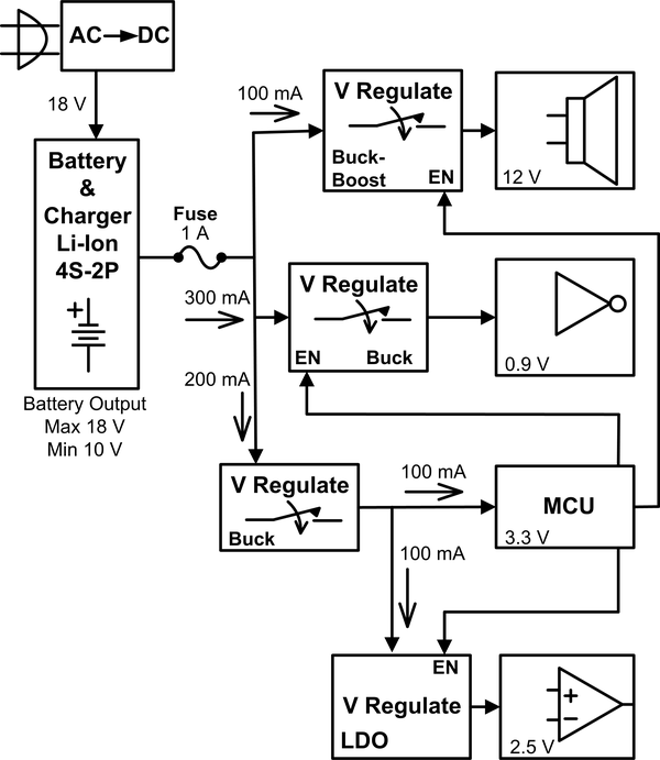
Figure 4-21. Multiple power supplies: battery and charger example
Both rechargeable battery systems and disposable batteries will have similar needs to remain functional over a wide variance in the supply voltage.
Including Power Supply Monitors
A useful addition to the power control system is the capability to monitor the voltages out of the regulators. Adding a voltage divider to an output voltage (Figure 4-22) and feeding that back to an analog-to-digital converter (ADC) port available on the host MCU can be useful in checking power sources or assisting in a sequenced power on/off cycle. The voltage divider (R1, R2) exists to scale Vout down to the midscale range of the ADC in the MCU.
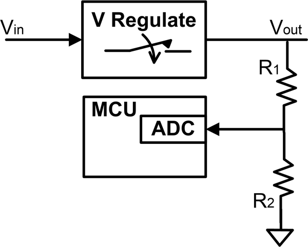
Figure 4-22. Monitoring power supplies
Power Bypass, Decoupling, and Filtering
Many of the multipurpose MCUs on the market have some limited analog capability, such as ADC ports. Some of these controllers separate the power with both digital and analog power connections. This provides a good opportunity to clarify the difference between a bypass capacitor and a decoupled power connection (Figure 4-23).
Frequently, the analog supply pins can be locally decoupled. Do this by using a ferrite bead and then both low-frequency bypass (Calf) and high-frequency bypass (Cahf) directly at the pin. A damped low-pass power filter can be used in place of the ferrite bead if greater rejection of power input noise is needed.
Figure 4-23 illustrates the difference between the bypassing and decoupling of power connections. The two terms are often interchanged or used incorrectly. Here, the capacitors (Cdlf, Cdhf) bypass the Vpower to maintain high-frequency stability. The combination of the ferrite bead (FB-LQ) and capacitors (Calf, Cahf) serves as a low-pass filter (LPF) to decouple the analog power pin from the digital switching noise present on the Vpower node. Decoupling involves series impedance in the power connection, and it can be useful in situations where the decoupled load does not need heavy transient currents.
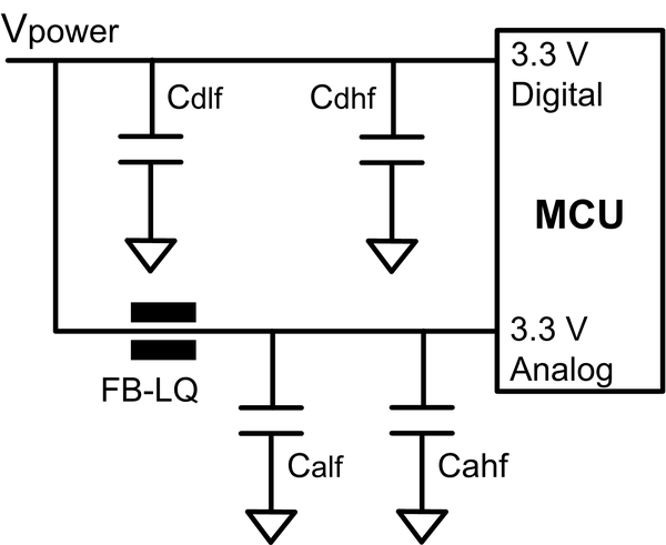
Figure 4-23. MCU power, bypass digital, decoupled analog
Radiated Noise Reduction: RC Snubbers, Ferrites, and Filters
In addition to switching regulators creating somewhat noisy power, they will also inject noise back into the power source they are fed from. Implementation of many switching converters involves components (Figure 4-24) to reduce the high-frequency noise that they pump onto the power grids, thus radiating electromagnetic interference (EMI).
In this example, both input and output have an LPF with a ferrite bead (FB1, FB2), and suitably sized high-frequency capacitors on both sides of the ferrite bead. If more isolation is required, an RLC network-damped low-pass network can be substituted.
In addition to the input/output filtering, an RC snubber (Rsnub, Csnub) is placed at the switched node. The RC snubber provides a low-impedance grounding path for high-frequency noise generated at this switched node (FDI: EMI & ESD).
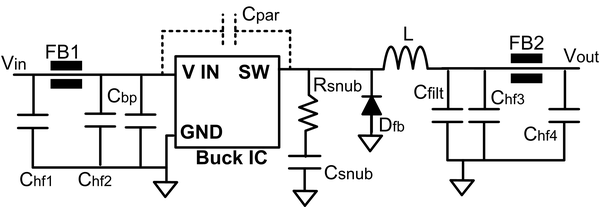
Figure 4-24. Noise reduction using snubbers and ferrites
Specific values for the RC snubber are dependent on converter frequency and internal transistor sizes. Switching converter manufacturers should provide suitable component values for their devices.
Power Output Noise Reduction: Damped LPF Networks and Cascaded Regulators
Higher-order filtering may be needed in some situations. For an in-depth design approach to damped low-pass filtering methods, Tompsett outlines a detailed design methodology; see “Further Reading”.
Other approaches here include using a switching converter, which is followed by a linear regulator that reduces noise further. This cascaded method allows a low-noise output while keeping the power losses associated with linear regulators minimized.
Power Grid Current Surges Due to Digital Logic
Figure 4-25 shows that the use of digital CMOS logic poses special challenges in keeping the DC power grid stable. The transition switching of any CMOS logic causes both NMOS and PMOS transistors to be on at the same time during the state transition. The result is a resistive short circuit between P&G on the state transition of every logic gate. This current spike, known as shoot-through, when replicated among the countless logic gates within any digital device creates both wideband EMI and high-frequency current demands on the power.
This is especially problematic due to I/O drivers inside a digital IC. The I/O has large transistors used in the I/O circuits of the chip, creating large shoot-through currents. The noise spectrum is distributed in frequency and is not just the fundamental clocking frequency, but includes many harmonics as well.
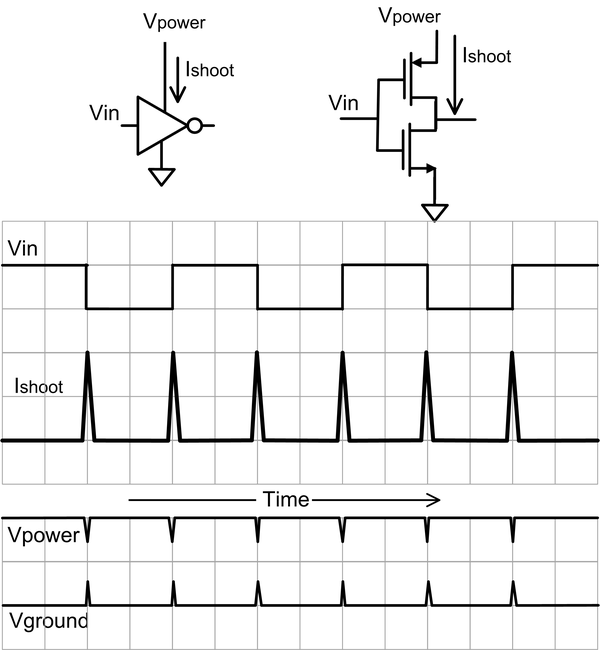
Figure 4-25. Digital current shoot-through
Due to shoot-through current, any impedance in the power or ground paths creates variance in the local P&G voltages. Low-impedance P&G planes are needed.
Low-Impedance Power and Ground Planes
Due to current surges, the impedance of P&G connections needs to be kept as low as possible. For that, dedicated P&G layers within the PCB are strongly preferred in all but the simplest of designs. Point-to-point interconnects will not suffice.
In Figure 4-26, Case A illustrates a hypothetical power interconnect with three different power values using point-to-point connections. Case B illustrates that all connections exhibit inductance and will cause the voltage across the power connection to vary dynamically as a function of any transient currents created by the devices being powered. Case C illustrates connecting the same points with a low-impedance connection. Placing this segmented power plane over a solid ground plane allows the capability to wideband-stabilize the power supply voltages with bypass capacitors.
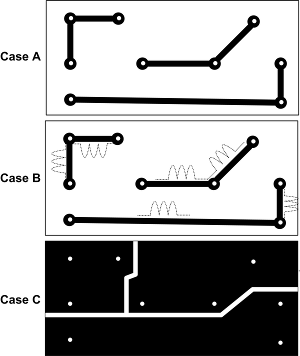
Figure 4-26. Power connections with low-inductance interconnect
Power Supply Bypass Filtering: Distributed Stabilization
In addition to the low-impedance interconnect strategy, the use of distributed bypass capacitance across the power plane (Figure 4-27) allows high-frequency stabilization of the power.
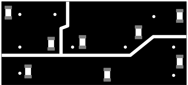
Figure 4-27. Distributed stabilization of power grid
Typically, stabilization of a power grid has three parts:
Bypass capacitors directly at all power pins on all ICs (at-chip bypass)
Bypass capacitance distributed across the power plane (grid bypass)
Bypass filtering at the voltage regulator output (regulator bypass)
A large PCB (e.g., a computer motherboard) with multiple high-speed digital chips must have all three of these. A small low-frequency PCB (e.g., a handheld remote for the TV) would be less demanding, and the grid bypass portion might be eliminated.
Bypass Capacitors at High Frequencies
The equivalent model for a surface mount multilayer ceramic capacitor (SMT MLCC) is shown in Figure 4-28. The elements are:
Cmain—Principle body of the capacitor
Cpar—Parasitic capacitance to the underlying PCB
ESR—Equivalent Series Resistance of the distributed device resistance
ESL—Equivalent Series Inductance of the device
Rleak—Leakage resistance between capacitance plates
The two important parameters for power bypass are ESR and ESL. The ESR limits the lowest impedance, and the ESL limits the maximum frequency where the device works effectively as a capacitor. These characteristics need to be considered in the selection of bypass capacitors.
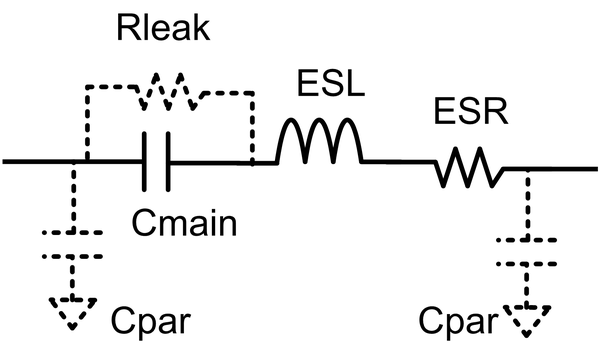
Figure 4-28. Equivalent model for high-frequency capacitors
Figure 4-29 shows the self-resonant characteristics of a typical surface mount capacitor. The low-frequency response is dominated by the Cmain capacitance and the high-frequency response is dominated by the ESL. In between, the device goes through self-resonant frequency (SRF) and the impedance drops to a minimum, which is equivalent to the ESR. The capacitor serves as a bypass filter beyond the SRF, but the effectiveness reduces with higher frequencies.
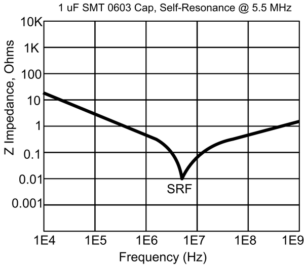
Figure 4-29. Self-resonance of capacitors
The presence of ESL limits the high-frequency capability of the device as a bypass filter for a power supply.
Table 4-1 shows a typical set of values for SRF as a function of capacitance value.
| Cvalue | SRF |
|---|---|
| 10 uF | 2.0 MHz |
| 1 uF | 5.5 MHz |
| 0.1 uF | 19 MHz |
| 0.01 uF | 57 MHz |
| 1000 pF | 180 MHz |
| 100 pF | 560 MHz |
| SMT MLCC, Package: 0603 (Imperial) | |
Ideally, bypass filtering needs to avoid frequencies where ESL dominates the impedance. The reality is that many designs have wideband current demands that go beyond the useful range of most capacitors. There are conflicting rules of thumb and empirical studies of how to deal with this issue. See “Further Reading”.
In theory, using capacitors with different SRF points connected in parallel circumvents the SRF characteristics of singular devices. This method is a common practice, but it is often blindly implemented without looking at the SRF of the capacitors. For this particular set of values, using capacitors 100X apart in value (such as 1 uF and 0.01 uF) would space the SRF apart in a suitable manner. Check the SRF of the specific devices used, because differences in manufacturer, dielectric type, or voltage rating can result in different SRF values.
The SMT body size can also affect ESL and SRF, with an SMT 0805 body having distinctly different characteristics than an SMT 1206 body. Some vendors also offer “low ESL” capacitors as an option. These devices usually have wider contact regions and shorter bodies, or they use multiple contact points to reduce inductance. Check the specific devices to be used for the details of their parameters.
Power Bypass Capacitor Value and Distribution
Bypass capacitors are utilized to do three separate things:
At-chip bypass is for the high-frequency current demands of an IC.
Grid bypass stabilizes local power grid connections and reduces voltage variance due to both connection impedances and bandwidth limitations of the power source (FDI: PCB).
Regulator bypass filters the power source (regulator) output and stabilizes the feedback control loop within the regulator.
Semiconductor vendors should provide their suggested devices for at-chip bypass to be used directly at their chips. If vendor information is not available, here are some suggested guidelines.
All power pins on all chips get dedicated bypass capacitors directly at the power pins.
At-chip bypass capacitors go on the same side of the PCB as the chip.
At-chip bypass capacitors should have minimal trace routing and use shortest-path connections. This is especially important with the wideband current demands of digital chips (FDI: PCB).
PCB layout should avoid/minimize vias in connections of at-chip bypass capacitors to minimize inductance (FDI: PCB).
Nothing smaller than 0.01 uF is suggested for at-chip bypass. Although smaller capacitance values have higher resonance points, frequently the smaller devices don’t exhibit low enough impedance or are insignificant in the mixed collection of impedances of the power grid (see Archambeault, 2007).
If possible, keep the SRF of the capacitor 10X above the most common frequency used in the IC. High-frequency chips will generally use the 0.01 uF minimum as described earlier. Some devices operating at lower frequencies may be able to use higher-valued bypass capacitors at the chip.
Using X5R and X7R capacitors is suggested due to their limited capacitance change (+/−15%) over temperature. Y5V devices exhibit extremely wide variance (+22%, −82%) and can be unpredictable.
NP0 and C0G capacitors exhibit little thermal and bias variance. However, these devices are limited in their capacitance values for a given volume device. Precise (<5% error) capacitance values are not needed for power bypass.
The voltage rating of capacitors should be greater than the maximum voltage seen in the circuit. A quick rule of thumb is 2X of the power supply that they are connected to.
Again, check with IC vendors for their preferred strategy for their chips.
The local power plane is kept stable with distributed capacitance.
Using many capacitors spread out is better than using a few capacitors.
The capacitors used for grid bypass are typically larger value than the capacitors used for at-chip bypass.
For a two-sided component-loaded PCB, put the grid bypass capacitors on the side of the PCB that is closest to the P&G layers. This minimizes inductance back to the P&G layers.
Distributed capacitance across the PCB should still use capacitors that exhibit good high-frequency characteristics, albeit resonating at a somewhat lower frequency than at-chip devices.
Using capacitors 100X larger in size than the at-chip bypass devices keeps the resonance points well separated. For the situation where at-chip bypass is 0.01 uF, this implies grid bypass capacitors of 1 uF.
Grid bypass capacitors should be distributed across the power planes such that any IC connected to the power plane has grid bypass in close proximity (Figure 4-30).
Multiple grid bypass capacitors are suggested near the perimeter of any high gate count logic IC (e.g., MPU, MCU, digital ASICs, FPGAs, memory ICs).
Using a thin insulating layer between P&G planes provides a negligible amount of grid bypass capacitance. This idea has been touted in various places but doesn’t hold up when examining the numbers (FDI: PCB, a quantitative example is examined there).
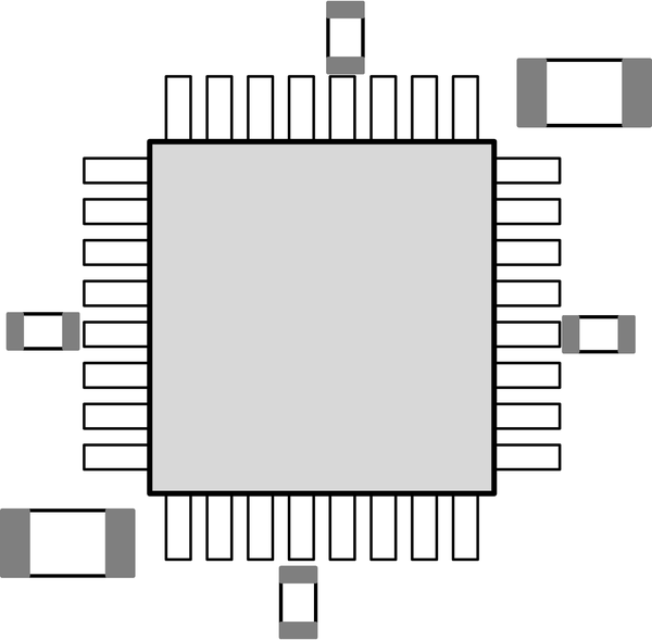
Figure 4-30. Bypass capacitance, at pin and across grid
Studies exist (see Bogatin, 2018) that deal with grid bypass capacitance as a controlled impedance versus frequency problem. Circuit simulators can analyze the interactive SRF of capacitors, but modeling the interconnection grid and everything connected to it is not quickly done. Typical design projects don’t have the resources to make such a detailed study. These guidelines are an approach that can be implemented efficiently.
Manufacturers of any voltage regulator should be able to provide their preferred configuration for regulator bypass and decoupling.
LDO regulators need to pay special attention to the ESR parameters of their bypass capacitors. Check the LDO specifications and application notes carefully.
Avoid electrolytic capacitors where possible due to their poor high-frequency response and long-term reliability issues. The aluminum electrolytic capacitor (AEC) is widely used in many products, but it is most often the first component to fail. Because the AEC can put a lot of capacitance into a small area at a low cost, it is widely used in consumer electronics.
SMT MLCC devices are preferred over AEC for their reliability and their low ESR/ESL.
Multiple SMT MLCC devices in parallel are a viable option for larger value capacitance.
Tantalum capacitors are more reliable than AECs and could also be used for regulator bypass.
If AECs are unavoidable, placing parallel SMT MLCCs with the AEC will improve high-frequency performance.
Summary and Conclusions
The important points of designing a power system are as follows:
AC power requires a strategy to avoid electric shock and ensure safety.
When the system fails, the device must remain safe. Understand and implement methods to avoid live contacts for both normal operation and any possible failure mode.
Overcurrent protection needs to be part of a weakest-link scenario. The fuse (or other protection) must open, not a PCB trace or an interconnect wire. This is a must-have for safety certification.
Internal AC power needs grounding or double insulated safety methods.
Off-line switchers for AC/DC conversion are efficient and compact DC power sources. Many low-cost options are available off the shelf, and it’s usually more cost-effective to purchase one instead of designing one from scratch. Look for devices that use internal self-protection circuits.
Regulate the power on the PCB where it is used. This minimizes problems due to connection impedance.
Switching DC/DC converters can provide voltage reduction, voltage boosting, or both, in a compact and efficient manner.
Linear regulators are inefficient, but they are useful where low noise on power or low EMI in the environment may be needed.
Digital logic creates high-frequency wideband surge currents on P&G.
P&G connections need dedicated PCB layers to create low-impedance connections.
Impedance of P&G connections needs to be minimized wherever possible.
High-frequency power stability requires bypass capacitors at all IC power pins.
High-frequency power stability requires distributed capacitance across the power grid.
Techniques for PCB layout of low-impedance connections are covered in further detail in Chapter 11. A carefully thought-out power system improves signal noise levels, reduces radiated EMI, and should remain smoke free when something in the system fails.
Further Reading
IEC 61140, “Protection Against Electric Shock,” https://www.iec.ch.
IEC 62368-1, “Audio/Video Information and Communication Technology Equipment – Part 1 – Safety Requirements,” https://www.iec.ch.
Bruce Archambeault, “Effective Power/Ground Plane Decoupling for PCB,” IEEE EMC, October 2007.
Switching Mode Power Supply Design, 3rd Edition, by A. Pressman, K. Billings, and T. Morey, 2009, ISBN 978-0-07-148272-5, McGraw-Hill.
High Speed Digital Design: A Handbook of Black Magic by H. Johnson and M. Graham, 1993, ISBN 978-81-317-1412-6, Pearson.
“Decoupling Techniques,” Analog Devices MT-101 Tutorial, https://www.analog.com/media/en/training-seminars/tutorials/MT-101.pdf.
Paul Brokaw, “An IC Amplifier User’s Guide to Decoupling, Grounding, and Making Things Go Right for a Change,” Analog Devices AN-202 Application Note, https://www.analog.com/media/en/technical-documentation/application-notes/AN-202.pdf.
Kevin Tompsett, “Designing Second Stage Output Filters for Switching Power Supplies,” Analog Devices, https://www.analog.com/en/technical-articles/designing-second-stage-output-filters-for-switching-power-supplies.html.
Vincent Greb, “Don’t Let Rules of Thumb Set Decoupling Capacitor Value,” EDN Magazine, September 1, 1995, https://www.edn.com/edn-access-09-01-95-dont-let-rules-of-thumb-set-decoupling-capacitor-value.
Jerry Twomey, “Simple Grounding Rules Yield Huge Rewards,” Electronic Design Magazine, April 27, 2012, https://www.electronicdesign.com/technologies/industrial/boards/article/21795841/simple-grounding-rules-yield-huge-rewards.
“Publications and Patents Authored by Jerry Twomey,” Effective Electrons, https://effectiveelectrons.com/articles-patents.
“Pentium III Processor Power Distribution Guidelines,” Application Note, Intel, April 1999, https://www.intel.com/design/PentiumIII/applnots/24508501.pdf.
Signal and Power Integrity Simplified, 3rd Edition, by Eric Bogatin, 2018, ISBN-13, 978-0-13-451341-6, Pearson Education.
Get Applied Embedded Electronics now with the O’Reilly learning platform.
O’Reilly members experience books, live events, courses curated by job role, and more from O’Reilly and nearly 200 top publishers.

