October 2011
Intermediate to advanced
354 pages
9h 30m
English
4
Memory Design: System-on-Chip and Board-Based Systems
4.1 INTRODUCTION
Memory design is the key to system design. The memory system is often the most costly (in terms of area or number of die) part of the system and it largely determines the performance. Regardless of the processors and the interconnect, the application cannot be executed any faster than the memory system, which provides the instructions and the operands.
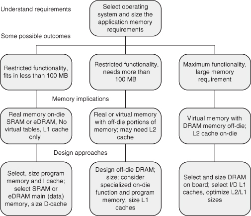
Memory design involves a number of considerations. The primary consideration is the application requirements: the operating system, the size, and the variability of the application processes. This largely determines the size of memory and how the memory will be addressed: real or virtual. Figure 4.1 is an outline for memory design, while Table 4.1 compares the relative area required for different memory technologies.
TABLE 4.1 Area Comparison for Different Memory Technologies
| Memory Technology | rbe | KB per Unit A |
| DRAM | 0.05–0.1 | 1800–3600 |
| SRAM | 0.6 | 300 |
| ROM/PROM | 0.2–0.8+ | 225–900 |
| eDRAM | 0.15 | 1200 |
| Flash: NAND | 0.02 | 10,000 |
Figure 4.1 An outline for memory design.
We start by looking at issues in SOC external and internal memories. We then examine scratchpad and cache memory to understand how they operate and how they are designed. After that, we consider the main memory problem, first the on-die memory and then the conventional dynamic RAM (DRAM) design. As part of the design of large memory ...
Read now
Unlock full access


