Chapter 4
ESD Power Clamps
4.1 ESD Power Clamps
In this chapter, ESD power clamp networks will be explored. ESD power clamp usage began in the mid-1990s, and today is a common practice of semiconductor chip design and ESD design synthesis [1–52]. Development of ESD power clamps and the synthesis into the semiconductor chip architecture is part of the ESD design discipline and an essential component of the art of ESD design. This chapter will focus on the classification of the ESD power clamps, key design parameters, the ESD power clamp design window, trigger elements, clamp devices, and issues and problems with the ESD power clamp.
4.1.1 Classification of ESD Power Clamps
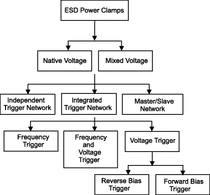
There are many different types of ESD power clamps, but conceptually they can be classified into different categories. Figure 4.1 shows a diagram of classification of ESD power clamps.
Figure 4.1 Classes of ESD power clamps

ESD power clamps must be tolerant of the power supply voltages observed in the functional semiconductor chip or system of chips [3–6]. ESD power clamps can be constructed for the native voltage power supply or mixed voltage power supplies. The ESD power clamps must be tolerant of the semiconductor chips they interface with, or the number of power rail voltages contained within a given chip.
Fundamentally, ESD power clamps contain some basic features. A first feature is the transfer of ESD ...

