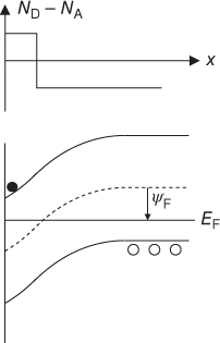
Figure 8.23 Doping profile and band diagram for MOSFETs with an n-type surface layer. The surface electric field is proportional to the slope of the bands at the surface, and is reduced in this structure.
8.2.10 Inversion Layer Electron Mobility
8.2.10.1 Mechanisms Affecting Inversion Layer Mobility
In the development of the current–voltage characteristics of the MOSFET in Section 8.2.3, we denoted the mobility of electrons in the inversion layer by the symbol ![]() . At inversion biases, electrons are confined to the oxide/semiconductor interface by the strong band bending in the semiconductor. The mobility of electrons in the inversion layer is lower than in the bulk semiconductor due to increased scattering at the oxide/semiconductor interface. Moreover, the mobility decreases with increasing gate voltage, since higher gate voltages increase the electric field confining electrons to the interface, resulting in increased scattering. The gate voltage dependence can be described by the empirical equation
. At inversion biases, electrons are confined to the oxide/semiconductor interface by the strong band bending in the semiconductor. The mobility of electrons in the inversion layer is lower than in the bulk semiconductor due to increased scattering at the oxide/semiconductor interface. Moreover, the mobility decreases with increasing gate voltage, since higher gate voltages increase the electric field confining electrons to the interface, resulting in increased scattering. The gate voltage dependence can be described by the empirical equation
where ![]() is the peak mobility at threshold and is a parameter characterizing ...
is the peak mobility at threshold and is a parameter characterizing ...
Get Fundamentals of Silicon Carbide Technology: Growth, Characterization, Devices and Applications now with the O’Reilly learning platform.
O’Reilly members experience books, live events, courses curated by job role, and more from O’Reilly and nearly 200 top publishers.

