Chapter 4. Sequential Logic
In this chapter, we will cover what sequential logic is and, more specifically, what flip-flops are and how to use them. Sequential logic is important for controlling the flow of data through your design as well as improving efficiency by allowing different sections of combinational logic to operate independently. This chapter starts a new example project; you will create a circuit that can keep track of a running total. We will also introduce how to properly read external inputs and solve the challenges that can be associated with them.
It should come as no surprise that because combinational logic is a type of circuit that depends only on the current inputs, the other type, sequential logic, is a type of circuit whose output depends on not only the current inputs but also the sequence of previous inputs. This means that the circuit has some sort of memory to be able to keep track of what has happened before.
A basic example is a circuit that keeps a running total of numbers. Each cycle (we will define what a cycle is later), it adds the current input to the previous sum, but the previous sum isn’t an input. The circuit “remembers” it.
So how do we create circuits that can remember things? It’s quite simple: we need to have feedback loops. In the example of the running total, we would need to feed the previous output back as another internal input. In practice, it gets a little more complicated than that, though.
Feedback Loops and Flip-Flops
Take a look at the circuit in Figure 4-1.
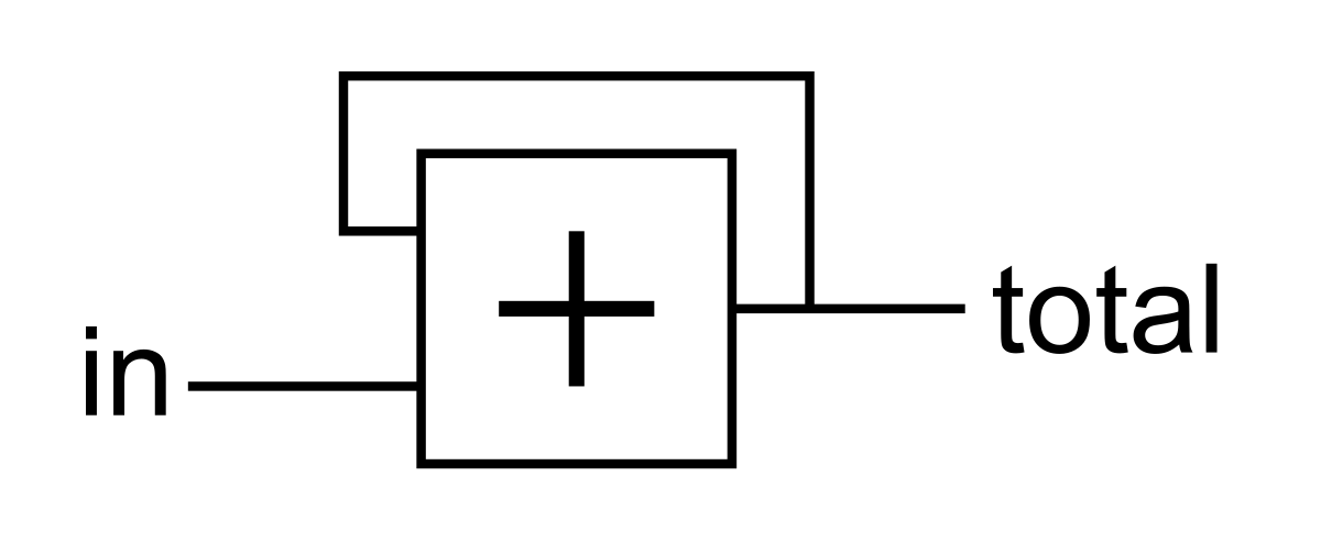
Figure 4-1. Running total circuit
In this diagram, the box with a + in it represents an adder. The two inputs on the left are the two numbers to be added, and the output on the right is the sum. In this example, we loop the sum back to one of the inputs. However, there is a problem. Imagine that somehow we know that total starts at 0. If we then change in to be 1, what is the output? Well, at first the two inputs are 0 and 1, so the output should obviously be 1. However, when the output is 1, the inputs are then 1 and 1, so the output should be 2. But if the output is 2, the inputs are 2 and 1, so the output should be 3. This will continue on forever.
If we built this circuit, how fast would total count up? Could we control the output at all? The speed it would count would be determinated by the incredibly short delay for the values to propagate through the logic gates. In practice, it wouldn’t even work. Binary numbers are represented with multiple bits, and the propagation delays for each bit would be different. This would lead to each bit updating its value at slightly different times, giving invalid intermediate values at the input, which would in turn lead to invalid outputs. The invalid outputs would cycle back to the input and produce more garbage. Basically, this is a mess and clearly not the way to keep a running total.
To make this work, we need a way to prevent the feedback from changing immediately. We need to be able to control how often it changes. Luckily, there is a circuit element known as the D-type flip-flop, or DFF, that will help us here.
Figure 4-2 is a basic representation of a common DFF. There are three inputs, D, clk, and rst, and a single output, Q. Before we get into how these work, we need to cover what a clock is.
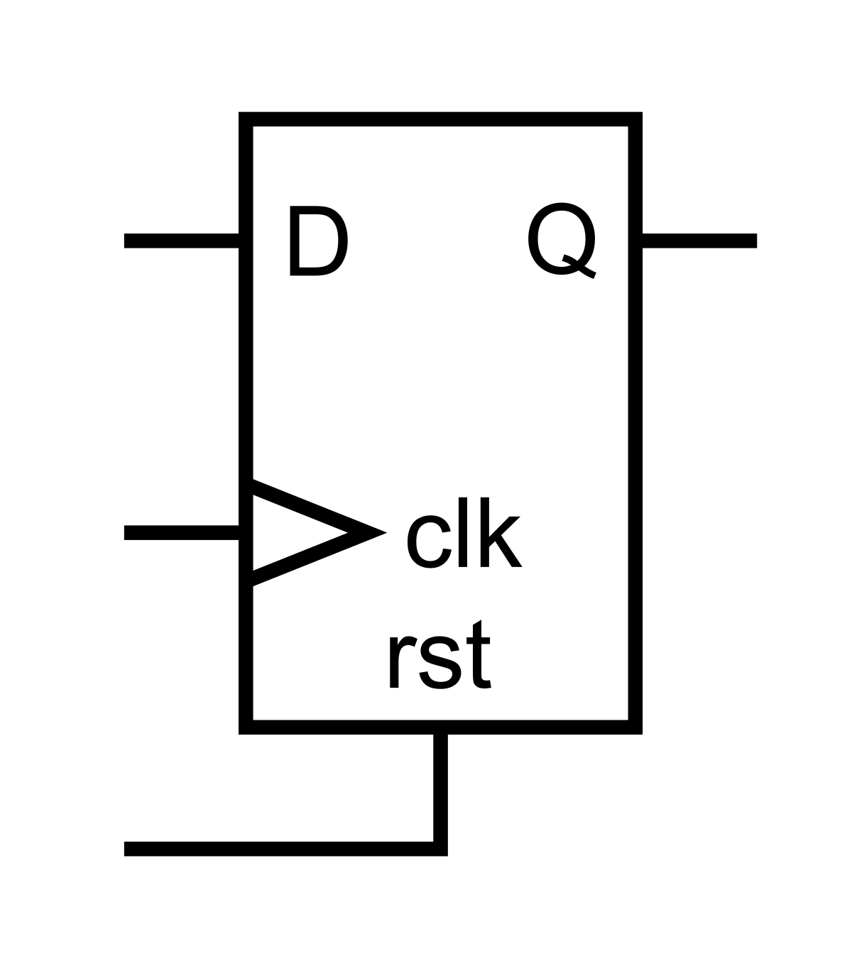
Figure 4-2. D-type flip-flop
Clocks
You have likely heard about clock signals before without even knowing about it. When you buy a computer, the spec sheet will always list the clock speed of the processor, something like 2.8 GHz. So what does this mean?
A clock is a signal that toggles between 0 and 1 with a set frequency. It looks something like Figure 4-3.

Figure 4-3. Clock signal
The important parts of the clock signal are the edges. There are two types: the rising and falling edges. Rising edges occur when the clock transitions from 0 to 1 and are marked with a little up arrow in Figure 4-3. Most of the time, the rising edge is the one you really care about. Falling edges occur the when the clock transitions from 1 to 0 and are used less often.
The time between edges is specified by the clock’s frequency. In the example of the computer processor running at 2.8 GHz, the clock will toggle 2.8 billion times a second, or once every 357 picoseconds! The clock on the Mojo isn’t quite that extreme. It runs at 50 MHz, meaning it toggles 50 million times a second, or once every 20 nanoseconds.
So back to the DFF. As you may have guessed, the clk input stands for clock. The function of a DFF is to copy the value from D and output it on Q on each rising edge of the clock. Between rising edges, if the value at D changes, the value at Q won’t change. Q changes only when there is a rising edge. In other words, the flip-flop will remember the last value of D and output it until it is told to remember a new value (at the next rising edge of the clock).
The input rst stands for reset and is used to force the output to a known value. In the case of our running total, we want the initial total to be 0. We can use the reset input to force the total to 0 when the circuit is powered on or needs to be reset. Without a reset, DFFs initialize to a random value.
The reset input usually forces the DFF to 0, but you can also have it set the DFF, forcing it to 1.
You will also sometimes see flip-flops drawn with another input called enable. This is used to select which rising edges the flip-flop should update on.
With your new knowledge of the DFF, take a look at the new running total circuit in Figure 4-4.
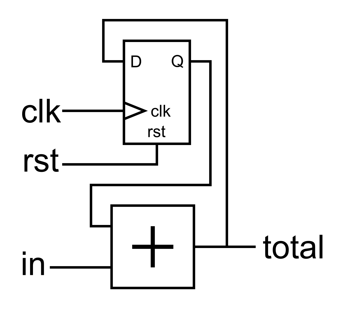
Figure 4-4. Running total circuit with DFF
The new circuit has two more inputs, clk and rst. The clock will dictate when the next value of in is added to total, and the reset input will allow us to reset the total to 0.
Now if we were to implement this circuit on the Mojo and use the switches as the input and the LEDs as the output, we couldn’t easily control it because it would add the input to the total 50 million times per second. Let’s go ahead and do it anyway to get a feel for using DFFs.
Create a new project based on the IO Shield Base and open up mojo_top.luc.
In Lucid, we have a type dff that we can use to instantiate DFFs in our design. Just as in the diagram, they have three inputs (clk, rst, and d) and one output (q). Since most of your design will use the same reset and clock signals, Lucid has a way to easily connect the same signal to many instances of DFFs or other modules:
  .clk(clk) {
    // The reset conditioner is used to synchronize the reset signal to the FPGA
    // clock. This ensures the entire FPGA comes out of reset at the same time.
    reset_conditioner reset_cond;

    .rst(rst) {
      dff running_total[24]; // Running total, 24 bits wide
    }
  }
Here we use the .port_name(signal_name){} syntax to connect clk and rst to the clk and rst inputs of the DFF. With this syntax, port_name is the name of the port on the instance. A port is simply an input, output, or inout of a module. In other words, signal_name is the name of the signal to connect to the port_name input of the DFF, in this case. It’s a little confusing here because the names of the input and signal are the same.
Also note that we nested the two port connection blocks. The module reset_cond won’t have rst connected because it isn’t in the block for that. However, running_total will have both rst and clk connected. You can list multiple connections for a single block by separating them with commas. For example, if we didn’t have reset_conditioner there, we could have instantiated the DFF as follows:
  .clk(clk), .rst(rst) {
    dff running_total[24]; // Running total, 24 bits wide
  }
Note that the port connection block syntax is great when you have a bunch of DFFs in your design, but if you have a single DFF, you could also connect only to that DFF with the following:
dff running_total[24] (.clk(clk), .rst(rst)); // Running total, 24 bits wide
You can mix and match any of these port connections to fit your needs. However, it is usually a good idea to set up a block that connects the clock and reset because they are used so much.
Also the rst input to the dff type is optional. If you don’t connect it, the dff won’t have a reset. If you don’t need a reset, don’t use it, as this will make your design easier for the tools to route. In the case of our running total, we definitely need a reset to be able to get the running total to a known value.
We can complete the design as follows:
module mojo_top (
    input clk,              // 50MHz clock
    input rst_n,            // reset button (active low)
    output led [8],         // 8 user controllable LEDs
    input cclk,             // configuration clock, AVR ready when high
    output spi_miso,        // AVR SPI MISO
    input spi_ss,           // AVR SPI Slave Select
    input spi_mosi,         // AVR SPI MOSI
    input spi_sck,          // AVR SPI Clock
    output spi_channel [4], // AVR general purpose pins
    input avr_tx,           // AVR TX (FPGA RX)
    output avr_rx,          // AVR RX (FPGA TX)
    input avr_rx_busy,      // AVR RX buffer full
    output io_led [3][8],   // LEDs on IO Shield
    output io_seg [8],      // 7-segment LEDs on IO Shield
    output io_sel [4],      // Digit select on IO Shield
    input io_button [5],    // 5 buttons on IO Shield
    input io_dip [3][8]     // DIP switches on IO Shield
  ) {

  sig rst;                  // reset signal

  .clk(clk) {
    // The reset conditioner is used to synchronize the reset signal to the FPGA
    // clock. This ensures the entire FPGA comes out of reset at the same time.
    reset_conditioner reset_cond;

    .rst(rst) {
      dff running_total[24]; // Running total, 24 bits wide
    }
  }

  always {
    reset_cond.in = ~rst_n; // input raw inverted reset signal
    rst = reset_cond.out;   // conditioned reset

    led = 8h00;             // turn LEDs off
    spi_miso = bz;          // not using SPI
    spi_channel = bzzzz;    // not using flags
    avr_rx = bz;            // not using serial port

    io_seg = 8hff;          // turn segments off
    io_sel = 4hf;           // select no digits

    running_total.d = running_total.q + io_dip[0];
    io_led =
      {running_total.q[16+:8], running_total.q[8+:8], running_total.q[0+:8]};
  }
}
Take a look at the line where we assign running_total.d. To access inputs and outputs of an instance, we use the dot (.) syntax. This line assigns the d input of running_total to the sum of the q output and the first eight switches. The next line simply connects the q output to the LEDs as we did before with result.
If you build and load this project onto your Mojo, when all the DIP switches are off nothing happens. However, the moment you flip the first switch, almost all the LEDs seem solid on except for the last few. This is because it is counting so fast we can’t see it. The first few LEDs are even pretty dim because the FPGA can’t fully turn on and off the LED that fast.
If you flip the DIP switches back to 0, you’ll freeze the counter at a specific value. Try this a few times just to prove to yourself that it is counting. If you turn on a few of the switches, it will count so fast you can’t see any of the LEDs blinking.
Timing and Metastability
When thinking about designs, it is easiest to assume that the DFF takes an instantaneous snapshot of its input at the rising edge of a clock. However, that isn’t true in practice. The DFF requires that its input doesn’t change for a small period of time around the rising edge of the clock.
The time required for it to be stable before the rising edge is known as the setup time, and the time after the edge is known as the hold time.
During the time around the edge, if the D input changes, the value of Q is not guaranteed to be valid. However, it gets worse. Not only can Q not be the value that D was, but it also can do some weird things such as oscillate between 0 and 1 or even get stuck somewhere in the middle. This instability can then propagate through your design, making other DFFs unstable.
In Figure 4-5, D is stable through the setup and hold times of the first two edges, so Q properly copies the value of D. However, on the last edge, D changes during the setup time, so the value of Q is unknown.
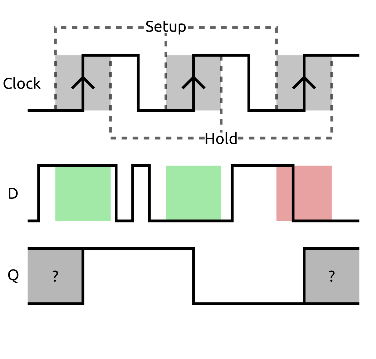
Figure 4-5. Setup and hold times of a DFF. D is valid for the first two edges, but violates the setup time on the last edge.
So how do we make sure that our designs don’t violate the flip-flop’s timing requirements? For the most part, the tools take care of it. Let’s look at an example of two flip-flops connected by an inverter, as shown in Figure 4-6.
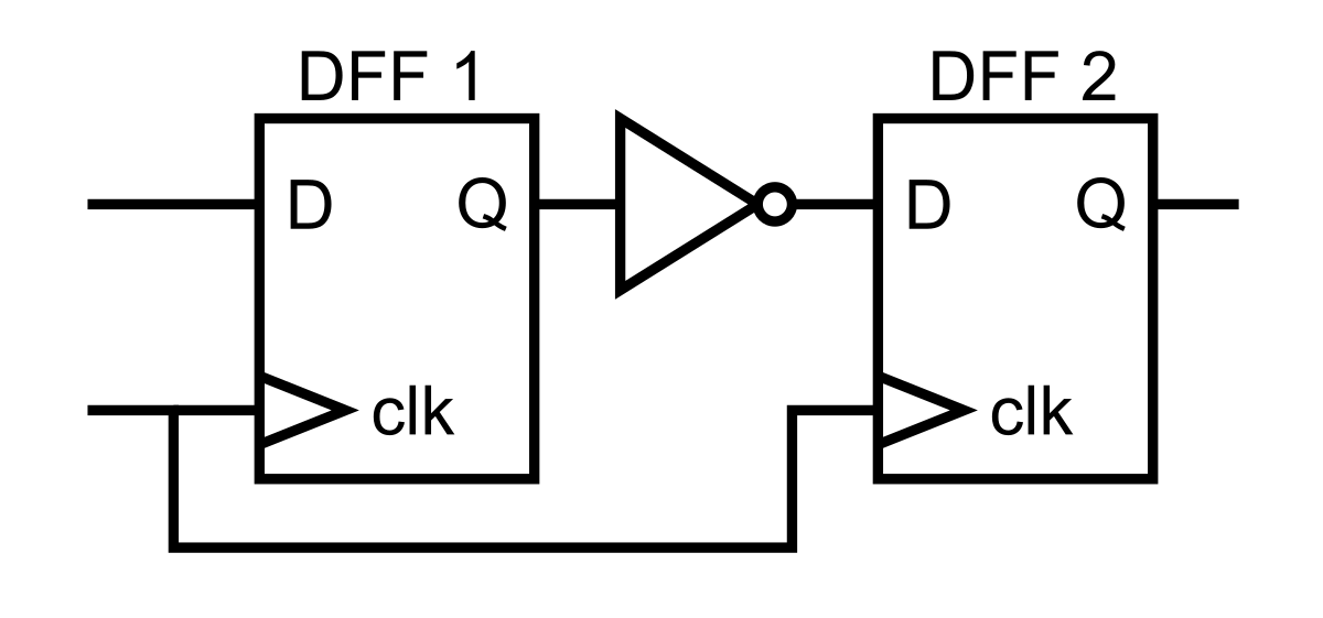
Figure 4-6. Two DFFs connected through an inverter
So what will happen here when Q of the first flip-flop is 0, but D is 1 and there is a rising edge?
Let’s quickly define the terms that you haven’t seen yet. If you look back at the schematic for this simple circuit, you’ll see that both DFFs have the same clock. It’s common for all the DFFs in your entire design to have the same clock. However, the DFFs are in different locations, and the clock signal originates from a single point. It takes time for the clock signal to reach each DFF. The difference in arrival time of the clock leads to clock skew. This means that the rising edges of the clock are not exactly the same for each DFF. Also note that the skew can be both positive and negative, depending how the circuit is actually laid out.
In Figure 4-7, Clock 1 refers to the clock seen at the input of DFF 1, and Clock 2 refers to the clock seen at DFF 2. Both clocks originate from the same source.
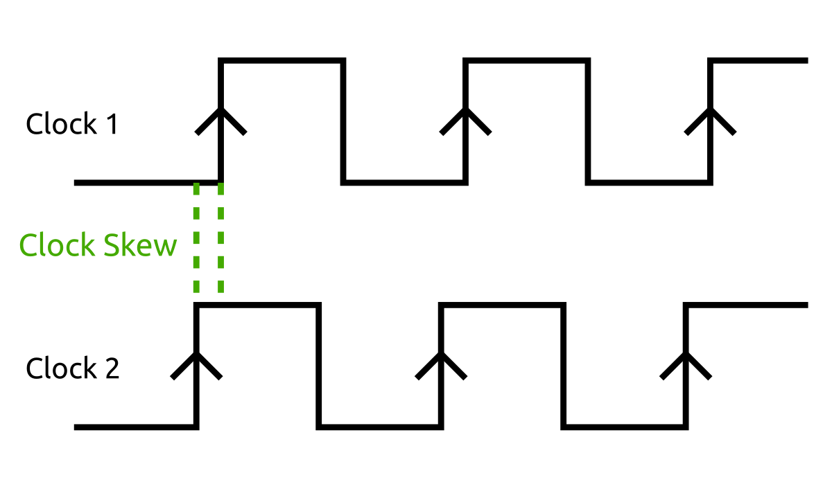
Figure 4-7. Clock skew
Earlier we also assumed that the DFF copied the D value to Q immediately at the rising edge. However, that’s not the case. There is a small amount of time between the rising edge and when Q actually changes. This is known as the clock-to-Q propagation delay, as shown in Figure 4-8.
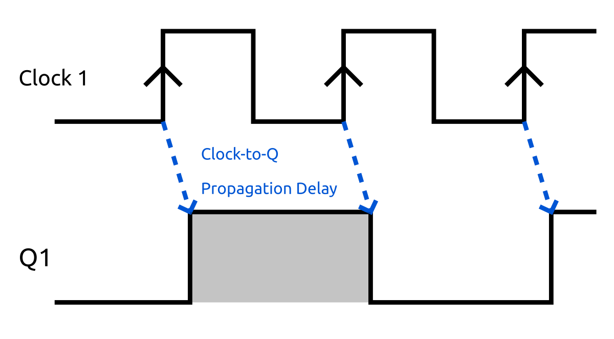
Figure 4-8. Clock-to-Q delay
Once Q changes, the new value needs to propagate through the circuit. The time it takes for the old value to be contaminated with the new value is called the contamination delay.
However, after the contamination delay, the value may toggle a few times before settling on the correct value. The time it takes after Q changes to when the output is stable and correct is called the combinational logic propagation delay. This delay is a function of your circuit design. The more logic you stick between two flip-flops, the longer this will be. It ultimately dictates the maximum clock speed at which you can run your design. Figure 4-9 illustrates contamination delay and combinational logic propagation delay.

Figure 4-9. Logic delays
If we ignore clock skew, to satisfy hold time we need to make sure that the clock-to-Q delay plus the contamination delay is equal to or greater than the hold time. Note that the clock-to-Q and the contamination delays are a function of how the circuit is laid out and not of the clock frequency. Because of this, we have to fully rely on the tools to make sure hold time is being met.
Again ignoring clock skew, to satisfy setup time, we need to ensure that the period of the clock minus the setup time is greater than or equal to the clock-to-Q delay plus the combinational logic delay. In this case, the period of the clock plays a role in timing. If for some reason the tools can’t meet timing on your design, they will prioritize satisfying the hold time over the setup time. This is because you can always satisfy the setup time by reducing your clock frequency (which increases the clock period).
Take a look at all of these constraints put together in Figure 4-10.
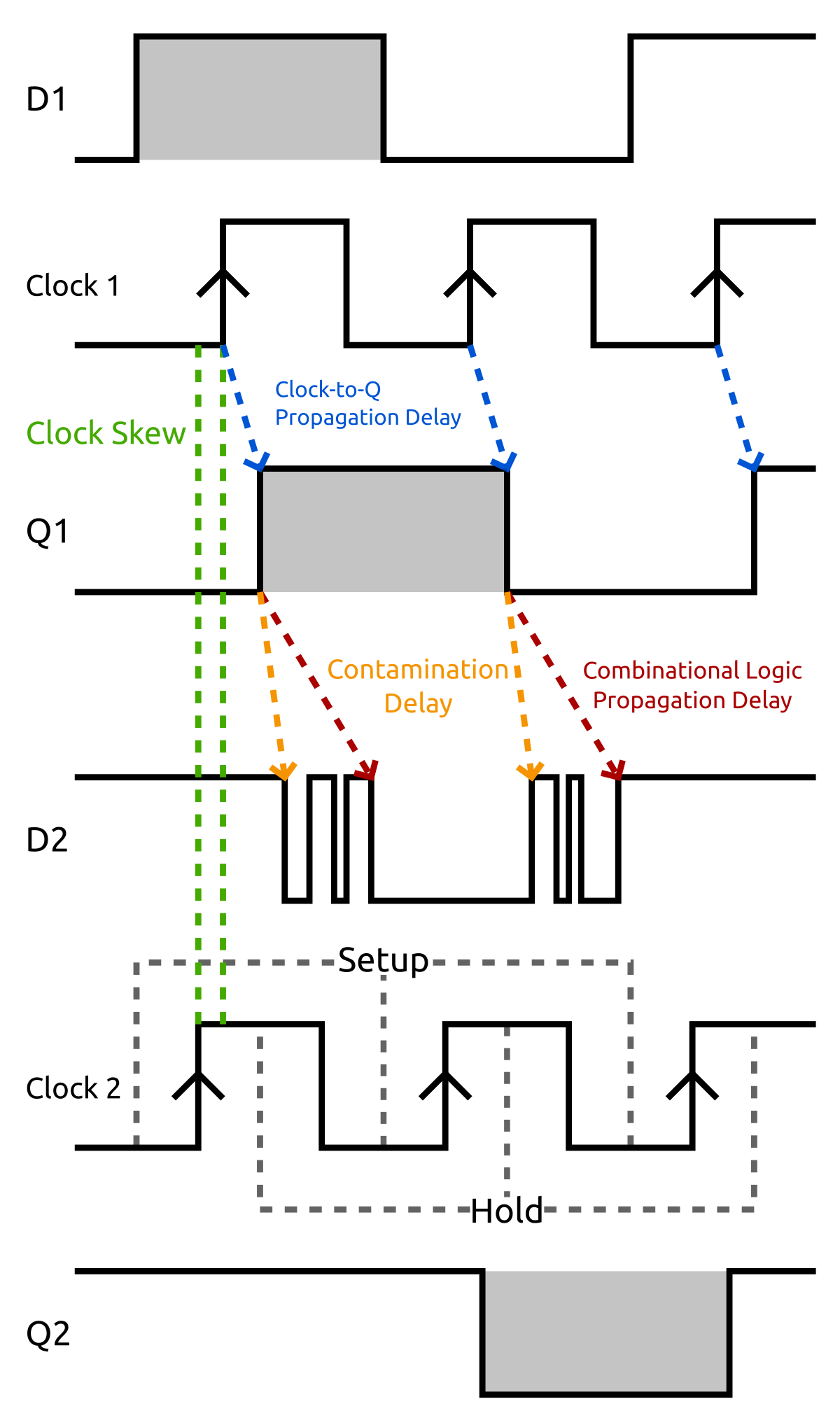
Figure 4-10. Timing of the DFF chain
Notice that in this example the circuit would be functional because the inputs to the flip-flops never change between the setup and hold times around each rising edge.
External Inputs
Luckily for us, the tools will figure out all these timing issues and attempt to lay out your design in such a way that it will all work. However, they can figure out the timing only when things are clearly defined. In some cases, the tools can’t satisfy timing for you. One case is when you have external inputs.
You can synchronize some external inputs to the system clock so that you don’t have to worry about the following issues. However, some inputs are generated from a different system clock or have no clock at all.
In fact, in our previous example with the counter, we used the DIP switches as an input directly to the counter. What happens if we flip one of the switches right on the rising edge of the clock? There is no way we can possibly synchronize our switch flips. This means we will eventually violate timing and cause stability issues if we flip it enough.
So how do we solve this issue? It is quite simple: we can use a simple circuit known as a synchronizer, shown in Figure 4-11.
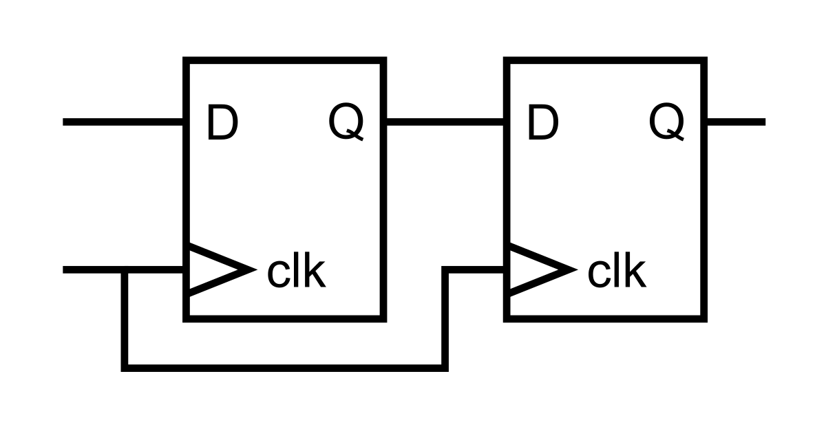
Figure 4-11. Basic synchronizer
The most basic synchronizer is two flip-flops connected together. You feed the unsynchronized input into the leftmost one, and the output on the right will be synchronized to the clock. This works because even if the first flip-flop becomes unstable, it is pretty unlikely that it will also cause the next to become unstable. However, there is still a chance that they both become unstable. To further reduce the possibility of instability, you can chain more than two DFFs together. The more you chain, the lower the probability of instability at the end. However, the payoff quickly diminishes after just two. This is something that all unsynchronized inputs in any digital system suffer from, and there is always that small chance that a value will be read incorrectly, or worse, the instability propagates. However, systems are designed so that their mean time between failures, or MTBF, is ridiculously high. Even just two flip-flops chained like this can have an MTBF of millions of years, depending on the input and flip-flop characteristics.
Add the Components
Open the Components Library, and go to Project → Add Components. We need three of the components for this project: the Pipeline, Edge Detector, and Button Conditioner. All of these can be found under the Miscellaneous category, as shown in Figure 4-12.
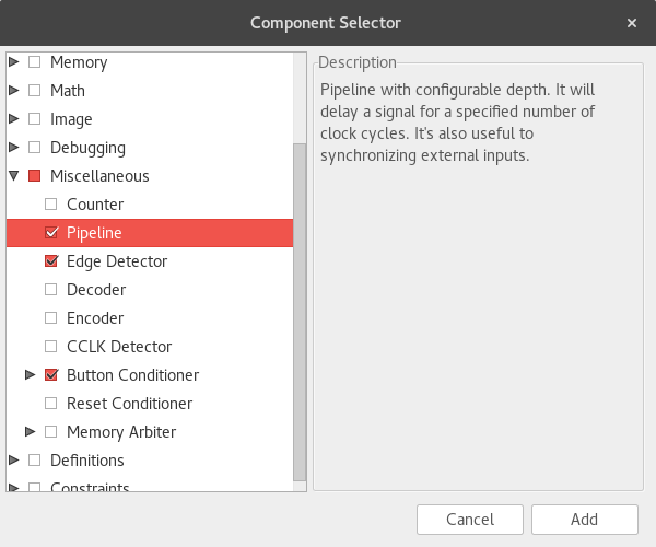
Figure 4-12. Components Library
The Pipeline component is simply a chain of DFFs like the synchronizer. The length of the chain is configurable using parameters. Let’s take a look at the source:
module pipeline #(
    DEPTH = 1 : DEPTH > 0 // number of stages
  )(
    input clk,  // clock
    input in,   // input
    output out  // output
  ) {

  dff pipe[DEPTH] (.clk(clk));
  var i;

  always {
    // in goes into the start of the pipe
    pipe.d[0] = in;

    // out is the end of the pipe
    out = pipe.q[pipe.WIDTH-1];

    // for each intermediate state
    for (i = 1; i < DEPTH; i++)
      pipe.d[i] = pipe.q[i-1]; // copy from previous
  }
}
The parameter DEPTH is used as the size of the array of DFFs, pipe. Even though DEPTH can take different values, it is constant at synthesis time, so you can use it as array sizes and indices.
Looking in the always block, the first line connects the input, in, to the first dff in the chain. The second line connects the output, out, to the output of the last flip-flop. To index the last flip-flop, we use the WIDTH attribute of the array. The WIDTH attribute for a single-dimensional array is simply a number. In this case, it will be the same value as DEPTH. For multidimensional arrays, WIDTH will be a single-dimensional array with each entry being the width of a different dimension. For example, dff array[3][5] will have a WIDTH attribute of {5, 3}, so that array.WIDTH[0] is equal to 3, and array.WIDTH[1] is 5.
There is a new type used in this module too, var. This stands for variable and is used to store a value that won’t really be in the hardware design but is useful in the description. The most common use for a var is as the index of a for loop.
Now let’s take a look at the for loop:
    for (i = 1; i < DEPTH; i++)
      pipe.d[i] = pipe.q[i-1]; // copy from previous
For loops take a similar form to C/C++ or Java for loops. They have the syntax for (init_expr; condition_expr; operation) statement. Only the type var should be used in for loops. The init_expr sets the initial value of the var—in this case, 1. The condition_expr is evaluated before each iteration to see whether the loop should continue. Finally, operation specifies how the var will change on each iteration.
Loops in Lucid my seem similar to software for loops you might be familiar with. However, they are implemented differently. for loops should be thought of as shorthand for writing everything out. The synthesizer will essentially unroll the for loop, duplicating the hardware required for each iteration. Unlike code, they don’t make your design any smaller. They only make the design files smaller and easier to maintain.
In this case, we couldn’t unroll the loop by hand because the number of iterations is specified by the parameter DEPTH. However, DEPTH is a constant (although it may have different values for different instances), so the tools can unroll it. for loops can be used only when they have a constant number of iterations that can be determined at synthesis time.
This for loop will simply connect the output of the previous flip-flop to the input of the next, creating the chain. Note that if DEPTH is 1, which is allowed with our constraint, the for loop will be ignored because the condition_expr will fail on the first iteration. This is what we want, because the input and output of the single dff would already be connected to the module’s ports.
Take a look at Figure 4-13 to see how this will look in hardware.
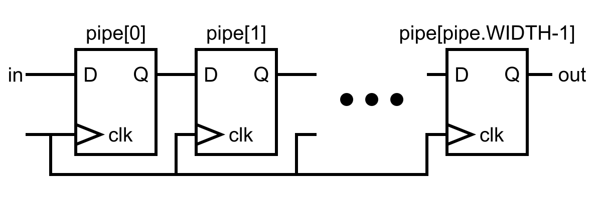
Figure 4-13. Hardware pipeline
Instantiating a Module
Now that you have a solid understanding of the pipeline component, let’s use it in the running total project to synchronize the switch inputs with the clock:
module mojo_top (
    input clk,              // 50MHz clock
    input rst_n,            // reset button (active low)
    output led [8],         // 8 user controllable LEDs
    input cclk,             // configuration clock, AVR ready when high
    output spi_miso,        // AVR SPI MISO
    input spi_ss,           // AVR SPI Slave Select
    input spi_mosi,         // AVR SPI MOSI
    input spi_sck,          // AVR SPI Clock
    output spi_channel [4], // AVR general purpose pins
    input avr_tx,           // AVR TX (FPGA RX)
    output avr_rx,          // AVR RX (FPGA TX)
    input avr_rx_busy,      // AVR RX buffer full
    output io_led [3][8],   // LEDs on IO Shield
    output io_seg [8],      // 7-segment LEDs on IO Shield
    output io_sel [4],      // Digit select on IO Shield
    input io_button [5],    // 5 buttons on IO Shield
    input io_dip [3][8]     // DIP switches on IO Shield
  ) {

  sig rst;                  // reset signal

  .clk(clk) {
    // The reset conditioner is used to synchronize the reset signal to the FPGA
    // clock. This ensures the entire FPGA comes out of reset at the same time.
    reset_conditioner reset_cond;

    // create a 3x8 array of pipelines with a depth of 2
    pipeline switch_cond[3][8] (#DEPTH(2));

    .rst(rst) {
      dff running_total[24]; // Running total, 24 bits wide
    }
  }

  always {
    reset_cond.in = ~rst_n; // input raw inverted reset signal
    rst = reset_cond.out;   // conditioned reset

    led = 8h00;             // turn LEDs off
    spi_miso = bz;          // not using SPI
    spi_channel = bzzzz;    // not using flags
    avr_rx = bz;            // not using serial port

    io_seg = 8hff;          // turn segments off
    io_sel = 4hf;           // select no digits

    switch_cond.in = io_dip; // connect the raw switch input to the conditioner

    // use the conditioned switch input
    running_total.d = running_total.q + switch_cond.out[0];
    io_led =
      {running_total.q[16+:8], running_total.q[8+:8], running_total.q[0+:8]};
  }
}
To instantiate the module, we use its name followed by the name of our instance. Note that the pipeline module has a clk input but not a rst input. This means we can put in the port connection block for clk, but not with running_total in the rst port connection block.
We also need the pipeline to be an array of pipelines. To do this, we can tack on the array size to the name. This will duplicate the pipeline module for each element in the array. Because the entire array is in the clk port connection block, each individual element will have its clk input connected to clk:
  .clk(clk) {
    ...
    // create a 3x8 array of pipelines with a depth of 2
    pipeline switch_cond[3][8] (#DEPTH(2));
    ...
  }
If you instantiate an array of modules and don’t connect a port at instantiation, that port will be packed into an array. This is what happens to switch_cond.in and switch_cond.out. While they are typically a single bit, because switch_cond is an array, they become 3 x 8 arrays themselves. This is convenient because we can then directly assign io_dip to switch_cond.in since they have the same dimensions. This also makes switch_cond.out a direct drop-in replacement for io_dip.
The default depth of the pipeline is 1, which is pretty useless because you could just use a DFF directly. We need to override this so that we get a chain of two DFFs. To specify a parameter’s value, you specify it basically the same way as you do a port connection, except instead of leading the name with a period (.), you use #. You can even add parameter values to port connection blocks if everything in the block has the same parameter name. If we didn’t instantiate the pipeline module in the port connection block, we could use the following:
pipeline switch_cond[3][8] (#DEPTH(2), .clk(clk));
The order of parameters and port connections don’t matter, but typically parameters are assigned first.
If you try changing DEPTH to an invalid value such as 0, you will get an error from the failing constraint:
Line 28, Column 13 : The constraint "DEPTH>0" for parameter "DEPTH" with value "0: {0}" failed
If you build and load this project, it should behave basically the same as before—except this time we don’t have to worry about metastability issues.
Checking Timing
How do we know that the tools were able to meet the timing requirements? If you look at the output when you build your project, a little bit above the end there is a section that looks something like this:
------------------------------------------------------------------------
  Constraint   | Check | Worst Case |  Best Case | Timing |   Timing
               |       |    Slack   | Achievable | Errors |    Score
------------------------------------------------------------------------
  TS_clk =     | SETUP |    14.461ns|     5.539ns|       0|           0
  PERIOD
  TIMEGRP
  "clk" 50
  MHz HIGH
   50%         | HOLD  |     0.447ns|            |       0|           0
------------------------------------------------------------------------


All constraints were met.
The important line here is the All constrains were met. part. This means the tools were able to route our design so that it should work under all operating conditions that the FPGA is designed to work in. If there was a problem, the Timing Errors and Timing Score columns would have nonzero values.
We will cover later what to do if timing fails, but for most designs running at 50 MHz, timing won’t be an issue. In the preceding case, the Best Case Achievable time of 5.539 ns means this design could run at 180 MHz (1/5.539 ns) without problems.
Also how do the tools know that the clock is 50 MHz? We told them! If you look under the Constraints section of the project tree, you will find a file called mojo.ucf. This file is where we tell the tools what pins on the FPGA to use for each signal internal to the Mojo as well as the frequency of the clock. The file io_shield.ucf contains the pin constraints used by the IO Shield.
Don’t worry about the user constraints file (UCF) details for now: we will get to them later.
Bouncy Buttons and Edges
We are going to modify the project further so that it adds the switch value only when we push a button. But first, you need to know some stuff about buttons. We could try to synchronize the button input as we did with the switches, but buttons have another issue: they often bounce when you press them. The contacts, instead of staying closed, hit each other and can then separate before slamming back together, as shown in Figure 4-14. This can happen a few times or none at all. To compensate for this, we need to register button presses only when they have been pressed and continue to be pressed for a small amount of time.
Luckily, the Button Conditioner component takes care of this for us.
Feel free to take a look at the contents of the module located in the button_conditioner.luc file. It works by first passing the button input through a pipeline, as we did with the switches. If the synchronized output is 1 (the button is assumed active high), a counter is incremented until it reaches its maximum value. When it reaches the maximum value, the button conditioner outputs 1. If at any point the button input is 0, the counter is reset and the output of the conditioner is 0.
The button conditioner will output 1 when the button is pressed, and 0 when it isn’t. However, we want to add the number only once for each time the button is pressed. To do this, we need to be able to detect when the button goes from 0 to 1. This is easy to do with a single DFF. You simply feed the value into the DFF. The output of the DFF will then be the value of the button from the last clock cycle. If the button was 0 on the last clock cycle, but is now 1, we know it was just pressed.
However, we don’t need to do this because another component does this for us: the Edge Detector component.
If you take a look at its source, you’ll see it does basically what was just described. The one main difference is that you can configure it so that it will detect rising, falling, or both types of edges using parameters.
Running Total
We now have all the pieces we need to make a more useful running total design.
First, we need to instantiate the button conditioner and edge detectors:
  .clk(clk) {
    // The reset conditioner is used to synchronize the reset signal to the FPGA
    // clock. This ensures the entire FPGA comes out of reset at the same time.
    reset_conditioner reset_cond;

    // create a 3x8 array of pipelines with a depth of 2
    pipeline switch_cond[3][8] (#DEPTH(2));
    button_conditioner btn_cond;
    edge_detector edge (#RISE(1), #FALL(0));

    .rst(rst) {
      dff running_total[24]; // Running total, 24 bits wide
    }
  }
Again, both of these don’t have rst inputs, so we can stick them in the clk port connection block. The default parameter values for the button conditioner are perfect, so we don’t need to override them. However, the edge detector needs to be told to look for only rising edges.
Finally, we need to connect it all up in the always block:
  always {
    reset_cond.in = ~rst_n; // input raw inverted reset signal
    rst = reset_cond.out;   // conditioned reset

    led = 8h00;             // turn LEDs off
    spi_miso = bz;          // not using SPI
    spi_channel = bzzzz;    // not using flags
    avr_rx = bz;            // not using serial port

    io_seg = 8hff;          // turn segments off
    io_sel = 4hf;           // select no digits

    switch_cond.in = io_dip; // connect the raw switch input to the conditioner

    btn_cond.in = io_button[4]; // io_button[4] is the "right" button
    edge.in = btn_cond.out;     // connect the button to the edge detector

    if (edge.out) // only add when the button is pressed
      // use the conditioned switch input
      running_total.d = running_total.q + switch_cond.out[0];

    io_led =
      {running_total.q[16+:8], running_total.q[8+:8], running_total.q[0+:8]};
  }
By using the if statement, we are able to assign running_total.d the new sum only when edge.out is 1. You may remember from before that under all circumstances, you need to assign a signal a value. The one exception to this rule is the d input of the DFF. This is because a DFF is able to save its last value, while a basic wire can’t. If you don’t assign it a value, the q output will stay the same.
Build and load the project onto your Mojo. By setting the DIP switches and pressing the “right” button, you can now add individual numbers to the running total. If you want to reset the total back to 0, press the button on the Mojo itself (not on the IO Shield).
Congratulations on completing the working running total design! This design is not only functional, but also quite robust, with all the proper precautions taken to clean up the external signals. You can try to connect io_button[4] to edge.in directly to see what kind of bad behavior you get when you use the external input directly. In my testing, the button press would be ignored about every third press. This obviously isn’t an issue of bouncing (which would cause multiple additions per press), so I must be violating timing and causing stability issues. A tricky thing with timing violations is that the behavior it can produce can seem random and unrelated to the input causing it (as the instability can propagate).
Get Learning FPGAs now with the O’Reilly learning platform.
O’Reilly members experience books, live events, courses curated by job role, and more from O’Reilly and nearly 200 top publishers.


