8.3 Detector Arrays 185
el. Allowing for atmospheric attenuation, non-normal solar incidence,
and a reasonable range of reflectances in an image reduces the average
expected flux to approximately 10^ photons/pixel for a "sunny" day
image. Light from a full moon, from the example in section 1.4, would
result in an average of about
10^
photons/pixel,
below the noise level of
the vidicon, and only a factor of two higher than the image orthicon
discussed in the previous section.
The sensitivity of the vidicon may be improved by using a return
beam read-out similar to that of the image orthicon. An even more sen-
sitive mode of operation for both the orthicon and the vidicon is the iso-
con return beam technique. During the initial time when electrons are
being replaced on the target surface by the electron beam, a fraction are
reemitted as secondaries and
scattered
over a reasonably large angle.
Once the correct negative charge is reestablished, the remaining beam
electrons are
reflected
in a narrow beam angle. By collecting and multi-
plying only the scattered electrons, the excess main beam shot noise is
therefore eliminated. We have not treated the important topics of retina
uniformity, beam focus and deflection techniques, and vidicon dynamic
range. These can be found in
(Csarba,
1985).
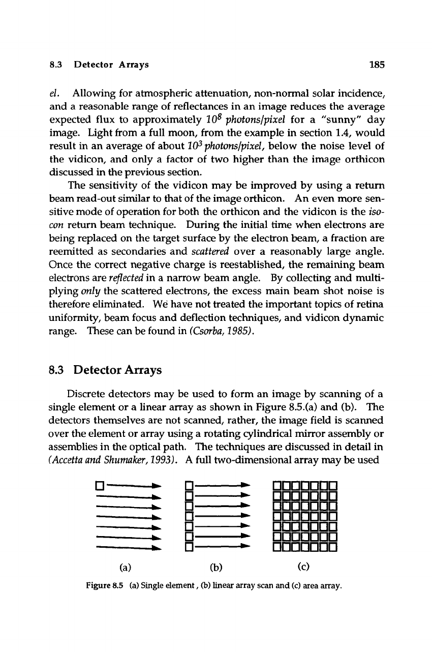
8.3 Detector Arrays
Discrete detectors may be used to form an image by scanning of a
single element or a linear array as shown in Figure
8.5.(a)
and (b). The
detectors themselves are not scanned, rather, the image field is scanned
over the element or array using a rotating cylindrical mirror assembly or
assemblies in the optical path. The techniques are discussed in detail in
(Accetta and
Shumaker,
1993).
A full two-dimensional array may be used
n • nnnnnnn
D ^ DDDDDDD
• • nnnnnnn
D-
D •
DDnnnDL
D ^ nannnnn
n ^ nnnnnnn
(a)
(b) (0
Figure 8.5 (a) Single element, (b) linear array scan and
(c)
area array.

186 Systems II.: Imaging
as shown in Figure 8.5(c). The single detector systenn uses standard
techniques for read-out, with the amplifier bandwidth determined by the
scan rate. Linear and area arrays may also be read out in parallel with
individual amplifiers and data recording for each pixel. Alternatively,
the parallel outputs from the amplifiers can be integrated, stored, and se-
quentially sampled to produce a serial data stream. In either case, de-
tector uniformity may seriously limit image quality and data reliability.
This problem can be overcome by calibration and the resultant stored
gain and bias adjustments for individual elements.
For large arrays, the complexity of individual detector amplifiers
may be overcome by the use of capacitive storage and sequential readout
of the detectors. The sampling shown schematically in Figure 8.6 may
be accomplished by a shift register-driven set of FET switches, but the
added capacitance of the output line increases the value of NEE. For
background-limited operation at long wavelengths, this is not a serious
problem; however, at near-infrared and visible wavelengths, the ampli-
fier noise becomes limiting. From Section
4.5,
the NEE is given by
8m
(8.7)
which, for a read-out line capacitance of 10 p/, a ^^ of 5 mS, y=l, and
a bandwidth of I MHz, becomes 250, if we use correlated double
sampling, that is, measure the voltage immediately before and after each
individual switch is closed, as discussed in Section
4.5.
Otherwise, kTC
noise results in a noise equivalent electron count given by
To integrating amplifier
)))))}
Figure 8.6 Schematic representation of array sequential read-out
Get Optical Sources, Detectors, and Systems now with the O’Reilly learning platform.
O’Reilly members experience books, live events, courses curated by job role, and more from O’Reilly and nearly 200 top publishers.

