Understanding Diodes
1 Silicon and germanium are semiconductor materials used in the manufacture of diodes, transistors, and integrated circuits. Semiconductor material is refined to an extreme level of purity, and then minute, controlled amounts of a specific impurity are added (a process called doping). Based on which impurity is added to a region of a semiconductor crystal, that region is said to be N type or P type. In addition to electrons (which are negative charge carriers used to conduct charge in a conventional conductor), semiconductors contain positive charge carriers called holes. The impurities added to an N type region increases the number of electrons capable of conducting charge, whereas the impurities added to a P type region increase the number of holes capable of conducting charge.
When a semiconductor chip contains an N doped region adjacent to a P doped region, a diode junction (often called a PN junction) is formed. Diode junctions can also be made with either silicon or germanium. However, silicon and germanium are never mixed when making PN junctions.
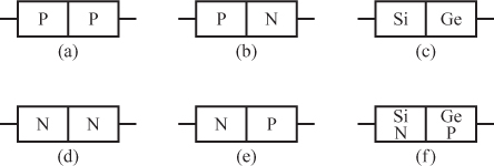
2 In a diode, the P material is called the anode. The N material is called the cathode.
Identify which part of the diode shown in Figure 2.2 is P material and which part is N material._____ ...
Get Complete Electronics Self-Teaching Guide with Projects now with the O’Reilly learning platform.
O’Reilly members experience books, live events, courses curated by job role, and more from O’Reilly and nearly 200 top publishers.

