Printed-circuit boards are
epoxy-bonded
fiberglass sheets, plated with copper.
The copperplating is etched away, leaving tracks (traces) that form
the interconnections of the circuit. PCBs are very reliable and are
the only option if you intend to produce more than one system. It is
possible to etch your own PCBs, but commercial PCB production
isn’t that expensive, and it is worth the cost to
get professionally produced boards.
EDA (Electronic Design
Automation) software is used to create the schematic and
PCB design. The most popular EDA software comes from Mentor Graphics
(http://www.mentor.com) and
Protel (http://www.protel.com).
There is also a GNU (http://www.gnu.org) PCB editor (called PCB)
that is freely available. Such programs normally come with several
tools, allowing schematic entry, netlist generation (a list of what
needs to be connected to what), PCB layout, manual routing (making
the connections), and autorouting. There’s a great
temptation to use autorouters, as they simplify the process of
generating the PCB by getting your workstation to do the hard work of
routing. However, I prefer to lay out the circuit board myself.
(I’ve seen some autorouters make a real
pig’s breakfast of a design.) Routing
the
board manually can take a long
while, but it is often worth the extra effort. It can also be very
absorbing, much like spending hours in deep meditation.
(It’s very Zen.)
PCBs can be single-sided (one layer), double-sided (two layers), or 4-layered, 6-layered, 8-layered, 12-layered, or more. The more layers you have, the easier it is to route your interconnections, but the costs of fabrication go up considerably with extra layers. Further, it’s much easier to debug a 2-layered board than a 12-layered board. With additional layers dedicated to power and ground planes, your system will have greater noise immunity. While not so critical for slow 8-bit systems, they are mandatory for high-speed computers.
Multilayered boards will be plated through, meaning that there will
be metallic connections through the holes in the board, connecting
traces of different layers together, as appropriate. A
solder mask
is the (normally) green coating on circuit
boards and prevents solder flowing between pads and tracks during
construction. It is possible to order commercial PCBs without
plating-through and without solder mask, but the small amount you
will save is not worth the hassle.
The overlay layers
(also known as silkscreen
layers
) are painted on and contain labels (such
as R30 or RAM4) showing component placement, used during
construction. The overlay layers are optional. If the boards are to
be manually populated with components by someone else, the overlay
layers are helpful during construction. If you’re
building them yourself, then you can easily do without the overlays
and save a few bucks.
Tip
A trick if you’re skipping the overlays is to place component information as text on the copper layers. Just be sure to avoid making contact with the circuit tracks!
The external copper layers are called top and
bottom (no surprises there). Traditionally, the
top layer was called the component
layer
,
and the bottom layer was called the solder
layer, since components used to be mounted on top, and
their pins soldered underneath. However, most modern circuit boards
place components on both sides and are soldered on both sides. Thus,
the terms “component layer” and
“solder layer” are seeing less use.
There are also internal copper layers for multilayer boards,
mechanical layers
(indicating any special physical
features), the keepout
layer
(showing the actual PCB shape), and
others. In four-layer boards, it is common practice to use the outer
layers for signals and the internal layers for power and ground. This
not only provides shielding, it also minimizes the current loop area,
thereby giving your design greater stability.
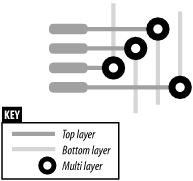
The five types of objects that can be placed on a copper layer are tracks, individual pads, components (arrays of pads grouped together), vias, and fills.
Tracks are used to interconnect components.
Track width is
expressed in thousands of an inch (mils) or in millimeters (mm).
Tracks can be of varying thickness, and often a PCB will have
different widths for different tracks. The fatter the track, the more
current it can carry. The thinner the track, the easier it is to fit
more tracks in a given space, therefore, the easier it is to route
the PCB. Table 4-1 gives a general guide to the
current-carrying capacity of different track widths (1 oz. copper),
for a temperature rise of +10 degrees C.
Table 4-1. Track width versus current flow
|
Mils |
mm |
Amps |
|---|---|---|
|
8 |
0.2 |
0.5 |
|
12 |
0.3 |
0.75 |
|
20 |
0.5 |
1.25 |
|
50 |
1.25 |
2.5 |
|
100 |
2.5 |
4 |
|
200 |
5 |
7 |
|
325 |
8.12 |
10 |
Check with the company doing your PCB fabrication as to what tolerances they can manufacture to. There’s no point in doing a PCB with 4 mil tracks if your local PCB fab company can only go as small as 8 mils.
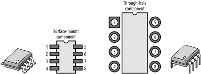
Pads are used to mount component pins,
and
they can be either round, rectangular, or oval. They consist of a
hole and a copper surround. A pad for a component in a DIP, for
example, will be a multilayered pad, meaning that the pad appears on
all copper layers, and the hole is drilled through the entire PCB. A
surface-mount component will have pads that appear on one layer only
(Figure 4-1). An array of pads grouped together to
form a component package is known as a
footprint. Surface-mount components have holes
of zero diameter (in other words, they aren’t
drilled). Surface-mount components are small with
“gull-wing” pins that mount flat on
the PCB. They are less susceptible to noise interference than the
older DIP style of packaging. However, DIP (through-hole) components
may be easily mounted in sockets and are therefore easily removed
during debugging. DIPs are sometimes preferable (although not always
feasible) during early development, while surface-mount is the only
option for production.
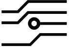
Tracks entering a pad should aim directly for the pad center, as shown in Figure 4-2 and not as in Figure 4-3.

When specifying the pads for a component, ensure that the pad size is large enough to accommodate the pins and to allow enough space onto which to solder. Also, ensure that the holes (for through-hole components) are large enough to take the pins. A standard DIP pin will happily go into a 0.7mm hole, while a DB connector requires 0.9mm holes for the signal pins and 3mm holes for the mounting pins.
Warning
Don’t assume that the libraries that came with your PCB CAD package have the pads, spacings, or holes right. It is not uncommon for CAD libraries to get it very wrong. (No kidding.) There’s nothing worse than getting a beautiful new PCB back and finding that you can’t insert the components! So, check and recheck.
When routing tracks around pads, ensure that there is sufficient
clearance, as shown in Figure 4-4. Tracks should
always change direction by 45-degree turns. Some PCB editing programs
allow you to do a
design rule check
(also known as an electrical rule check) to
ensure that correct clearances are maintained and that there are no
potential shorts. (It’s no guarantee that there
won’t be a problem, but it’s a
start!)
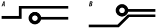
Avoid right-angle turns (A) and close passes (B), as shown in Figure 4-5.
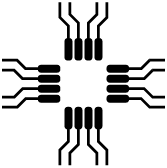
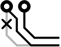
Closely spaced pads on surface-mount components can present a
problem. Often the tracks leaving a surface-mount device are too
close together to actually do anything with. The solution is to
fan out the tracks, thereby giving greater
spacing to the tracks. This is shown, in a simplified form, in Figure 4-6.
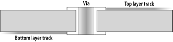
Vias are used to connect tracks on different
layers together (Figure 4-7). They are, in effect,
little pads. Vias can either be through-hole vias appearing on all
layers (Figure 4-8) or blind
or buried vias, appearing only on the layers
they are interconnecting and intermediate layers. Making the vias as
small as possible aids in routing the PCB, but check with your PCB
manufacturer as to how small you can go. Remember to ensure that the
outside diameter of the via is sufficiently bigger than the hole, so
that the entire via is not drilled out during fabrication. If space
permits, a useful trick is to make the vias with 0.4mm holes. That
way, if there is a bug in the PCB layout or a manufacturing fault,
you can use the vias to solder in wire-wrap wire, and manually make
(or remake) a connection.
Fills are used to provide shielding to certain
sections of the PCB and also for circuit paths that carry a lot of
current. Ground fills are commonly placed in and around analog
sections of the circuit to isolate them from digital crosstalk.
The first thing to note when laying out a PCB is that someone (or some robot) is going to have to assemble it. As tempting as it might be to cram everything into the smallest space possible, remember the limitations of whomever (or whatever) will be building it. That’s not to say you should make the PCB as big as possible; just be realistic. Also, don’t bring components and tracks right to the edge of the PCB. Leave a spacing of 5 mm (200 mils) around the outside. If your PCB is to go inside a case, or be mounted in some way, make sure that you have the dimensions correct, and don’t forget to add mounting holes.
There are two schools of thought in placing components (especially
integrated circuits) on a PCB. The first is that all components
should be placed with the same orientation. For instance, the pin 1
of each chip should point to the upper-left corner of the PCB. This
simplifies populating (or stuffing) the board
with
components, especially if this is to be done by a contract
manufacturer in an automated process. Having varying orientations may
add to the expense of production, if you’re not hand
assembling the boards yourself. Some people also think that this
makes a board look neater.
The second school of thought is that you orient the chips so as to optimize the routing process. The pinouts of different chips are not necessarily conducive to uniform orientation, and spinning one chip 90 or 180 degrees to its neighbor may greatly simplify the routing of tracks between the two. This can lead to a smaller board size, fewer vias, and shorter track lengths. This then results in lower PCB cost, less noise, less crosstalk, and better noise immunity, which is especially important in higher-speed systems.
Whatever you decide about orientation, group related components together. Put the voltage regulator and its support components near the power connector. Any analog circuitry (such as sensors or amplifier circuits) should be as far from this as possible. By placing chips into functional groups, routing is made easier. This may seem like obvious stuff, but it’s amazing how often it’s ignored.
The clocks and high-speed signals should be routed first, to ensure that they take the most direct path possible from source to destination. Wherever appropriate, place shielding (fills) to isolate these signals from other parts of the PCB. This should be done prior to routing other connections; otherwise, there may not be sufficient space later on. In particular, tracks should never be routed under or around crystals, oscillators, or any clock generation circuit, and these components should be isolated by fills (connected to ground) from the rest of the circuit. Crystals should lie flat against the PCB (rather than being mounted vertically), and a ground plane should be placed under them to shield from emissions.
For high-speed signals, make sure that there is a ground return path close to the track so that the current loop area is minimized. Allow as much space as possible between high-speed tracks. Having two rapidly changing signals in close proximity will result in crosstalk, and this will cause unreliable operation. Every track has an inherent impedance (resistance); although small, it can affect the transmission of fast signals. In particular, a via or sharp corner represents a change of impedance along the track, and this can cause signal reflections. Therefore, it’s important to keep the number of vias to an absolute minimum and avoid right-angle turns in tracks. If you need to make a track turn 90 degrees, use two 45-degree turns in succession.
In high-speed systems, you need power and ground planes that are continuous. In other words, you need planes that cover the entire PCB with no breaks. Any break in the power or ground plane makes the current loop area larger, and this can increase inductance and radiation. This means, for high-speed systems, you really need to use four or more layers on the PCB. For low-speed microcontrollers, you can get by without separate planes or by providing fills in and around components on the signal layers.
When routing buses (such as data and address), keep the tracks running parallel if possible (Figure 4-9). This is bad practice for clock signals, since it can induce crosstalk in neighboring tracks, but is appropriate for buses. The reason is that bus signals will change state together and will then hold that state until the next transaction. The device receiving the bus signals will sample their state only when they are stable (unchanging). Since crosstalk is generated on change-of-signal state, running parallel buses is not a problem. By keeping the bus tracks parallel, the signals travel approximately the same distance for each track. A track that takes a different path completely will have a trace-length mismatch, and this can increase signal skew, where the time it takes for a signal to propagate is shifted. This can adversely affect signal quality in high-speed systems.
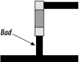
Stubs are short tracks that
leave
a main track to connect to a component (Figure 4-10). A stub represents an impedance mismatch for
a signal and can result in reflections. A better way is to place the
component so that the pad lies on the primary signal track (Figure 4-11).

All power and ground traces should be as fat as possible, and if feasible, separate power and ground planes (layers) should be used. The power ground (ground coming in with the power supply) should be separate from signal ground or digital ground (the ground running to all your chips), and both separate from the analog ground, if one is present. They should all be connected together, but only at one point. This helps isolate the digital and analog sections from each other’s noise, as well as from the power-supply noise.
Tip
A very useful and simple idea is to place a single pad in the middle of a ground plane (or fill), off to the side of the board. Solder in a post (or even a wirewrap pin), and use this to connect the ground lead of your oscilloscope probe. This can make the debugging process a lot less awkward. You must always use the ground lead of your oscilloscope probe. Without it, you can’t get an accurate picture of the timing and voltages of your signals. (Voltage is the potential difference between two points, so you must have a reference.) It’s very important.
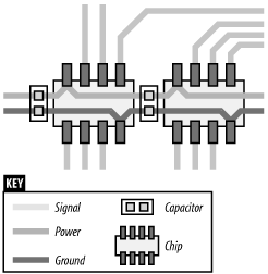
Decoupling capacitors should be as close as possible to each power pin of each integrated circuit. Figure 4-12 shows two components on a two-layer PCB, with power and ground tracks routed horizontally through the middle and decoupling capacitors placed close to the power pins.
Get Designing Embedded Hardware now with the O’Reilly learning platform.
O’Reilly members experience books, live events, courses curated by job role, and more from O’Reilly and nearly 200 top publishers.

