So, with all that in mind, let’s create a simple circuit board for an AVR computer. This design is covered in detail in Chapter 6, but for the moment, we’ll just use it as an example so that we can see the process of producing a printed-circuit board.
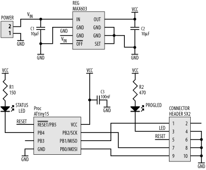
We start with the schematic (Figure 4-13). This design brings together the voltage regulator circuit, the AVR processor with a status LED, and the in-circuit programming interface.
Note that no connection is made for pin 2 of the connector. This is the +5V supply provided by the programmer. Since our embedded system has its own supply of +5V (VCC), the external source is not required. (If we were building a 3V version of this computer, then we would need to use the programmer’s +5V supply, and we’d have to disable the output from the voltage regulator during programming.)
From this design, we use our schematic editor to generate a netlist file, which tells the PCB editing software what interconnections need to be made.
Importing the netlist file into the PCB editor automatically loads the component footprints. These are manually rearranged to provide optimum placement, ensuring shortest track runs between components (Figure 4-14). Note how related components—such as the voltage regulator, C1, C2, and the power connector—are placed together. The silkscreen (overlay) layer shows the outline of the components. In this example, surface-mount components have been used for the resistors, capacitors, and LEDs, while the two integrated circuits are DIPs. Note the three-pad triangular LEDs. Only two of the pads are connected to the internal LED; the third is unused. This tiny circuit board measures just 2” by 0.6”.
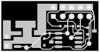
Once you’re satisfied with the component placement (and this may need tweaking as you go), the connections are routed. Figure 4-15 shows the PCB with manually routed connections. In this case, the overlay layer has been “turned off” for clarity. Note the use of fills for power and ground connections. For such a simple circuit, operating at low speed with no external system buses, the PCB layout is relatively trivial.
Just for comparison, Figure 4-16 shows the same board, but this time using an auto-router to make the connections. Note the bizarre track loop near pin 8 of the processor, the strange meandering track paths, and the unnecessary via in the middle of the PCB.
This is a simple board, so even an autorouter can make most of the connections. On complex boards, the average autorouter gives up about halfway through, after first making a complete mess. There are autorouters that do a much better job than this, but they are very expensive.
For greater noise immunity, a polygon plane is placed on the bottom layer of the manually routed PCB to act as a Faraday shield (Figure 4-17). Note how the polygon has “flowed” around the component pins, yet has connected to the ground pins. In this way, the polygon is a ground plane, providing a (small) degree of noise immunity for the system. The “void” region in the middle right is where it could not reach, due to the prerouted tracks. If designing a four-layer board, the polygon fill would be placed on a separate layer and should have no discontinuities at all, except where it flows around the pads of through-hole components.
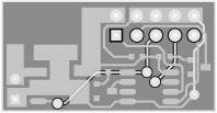
Using all surface-mount parts (where possible) makes the design even smaller. Figure 4-18 shows the same design (manually routed), but this time using surface-mount versions of the processor and regulator and even smaller-sized resistors and capacitors. The new board size is just 1” by 0.5”. The pads for the regulator are covered by fills and so are not apparent. (Once the PCB is fabricated, the pads stand out easily!) The only through-hole components are the power connector and the I/O connector. Note the four vias needed to route the tracks. For the previous design, the pads of the DIP components effectively acted as vias. On the all-surface-mount version, since just about everything is on the same layer, vias are required to take tracks to the bottom layer of the PCB.
You could make this board even smaller (perhaps 0.5” by 0.5”) by placing surface-mount components on both sides of the PCB. This adds to the cost of construction if you’re having it professionally done.
Figure 4-19 shows the surface-mount PCB, now with a Faraday shield.
Before sending off your circuit board design to be fabricated, print it out and carefully look at it. Check clearances to ensure that there are no potential shorts. Just because there’s a whisker gap between a track and a via on the screen doesn’t mean that there won’t be short there when it’s made. Give enough clearance to make this an impossibility. Good practice is to set your clearances to be equal to or greater than the minimum track width to which the PCB manufacturer can etch. Anything finer and you’re asking for trouble.
Tip
When your design is printed out, place the physical components on the paper and check for clearances. Just because the component outlines in the CAD package didn’t collide does not mean that the physical chips won’t. It is much easier to solve these problems before the PCB is fabricated than after.
Get Designing Embedded Hardware now with the O’Reilly learning platform.
O’Reilly members experience books, live events, courses curated by job role, and more from O’Reilly and nearly 200 top publishers.


