4.3 DESIGN PROCESS FLOW: THE PROGRAMMABLE LOGIC DEVICE ROUTE
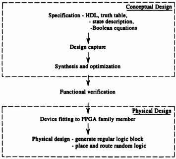
A typical programmable logic device (PLD) design process flow is shown in Figure 4–6. The starting specification might be informal and hand drafted in anything from an HDL to a collection of Boolean equations. Design capture moves the design into the CAD environment and requires the engineer to restate the creation for machine consumption. This might be preparing a file in a preferred notation or marking entries in a table. Synthesis and optimization uses algorithms to manipulate the logic design to improve it by exploiting don’t care states to minimize the number of gates used. Function verification may be a unit-delay simulator to generate circuit outputs, or may amount to a manual inspection of truth table data. Device fitting matches logic/gate demand and input/output (I/O) demand to part family members. Finally, physical design produces manufacturing data, a binary stream, for programming specific devices. This must be achieved by generating a layout of the required circuit in the chosen FPGA cell and wire scheme. It may amount to running a simple logic block generator or it may be placing and routing random logic using manual and automatic software tools.

Figure 4–6. PLD design process flow.
4.3.1 Conceptual Design of Display Driver
In the case of a CAL design the specification is given in Table 4–2. The minimization ...
Get Field-Programmable Gate Arrays: Reconfigurable Logic for Rapid Prototyping and Implementation of Digital Systems now with the O’Reilly learning platform.
O’Reilly members experience books, live events, courses curated by job role, and more from O’Reilly and nearly 200 top publishers.

