3.4 Three-phase PWM Voltage Source Inverter
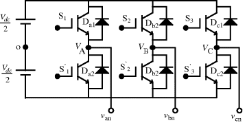
The power circuit topology of a three-phase voltage source inverter is shown in Figure 3.15. Each power switch is a transistor or IGBT with anti-parallel diodes. The pole or the leg voltages are denoted by a capital suffix letter VA, VB, VC and can attain the value +0.5 Vdc when the upper switch is operating and −0.5 Vdc when the lower switch is operating. The phase voltage applied to the load is denoted by the letters van, vbn, vcn. The operation of the upper and the lower switches are complimentary (a small dead band is provided in real time implementation).
Figure 3.15 Power circuit topology of a three-phase voltage source inverter
The relationship between the leg voltage and switching signals are
where ![]() when the upper power switch is ‘ON’ and
when the upper power switch is ‘ON’ and ![]() when the lower switch is ‘ON.’ If the load is assumed to be a star connected three-phase, then the relation between the phase-to-neutral load voltage and the leg voltages can be written as
when the lower switch is ‘ON.’ If the load is assumed to be a star connected three-phase, then the relation between the phase-to-neutral load voltage and the leg voltages can be written as
where is the voltage difference between the star point n of the load and the negative rail of ...
Get High Performance Control of AC Drives with Matlab / Simulink Models now with the O’Reilly learning platform.
O’Reilly members experience books, live events, courses curated by job role, and more from O’Reilly and nearly 200 top publishers.

