5.5 CMOS LOGIC GATES
Here we are going to use CMOS transistors, known as complementary MOS transistors, consisting of both PMOS and NMOS transistors. As for NMOS logic circuits, these CMOS logic circuits have pull-up and pull-down networks. However, for CMOS logic, the pull-up network consists of PMOS transistors. The functions realized by pull-up and pull-down networks are complementary to each other. The n-channel network is between the output and ground, and the p-channel network is between the output and VDD. The number of transistors in each network is equal to the number of inputs.
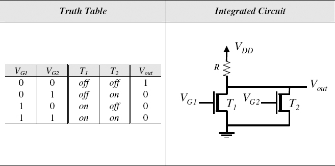
Figure 5.6 NMOS (Two-Input) NOR Gate and Its Truth Table
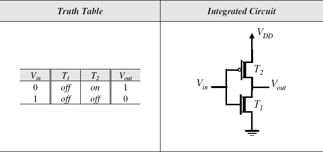
Figure 5.7 CMOS NOT Gate and Its Truth Table
5.5.1 CMOS Inverter
The circuit diagram for a CMOS inverter is shown in Figure 5.7. For the logic high input, transistor T1 will be turned on and T2 will be off, thus pulling down the output node to ground, resulting in logic 0 at the output. On the other hand, for logic 0 input, T1 will be off and T2 will be on, thus connecting the output node to the higher voltage, VDD. Notice that there is no protective resistance.
5.5.2 CMOS NAND Gate
A CMOS (two-input) NAND gate is shown in Figure 5.8. For this network, if all the inputs are high, the NMOS transistors will be on, the PMOS transistors will be ...
Get Introduction to Digital Systems: Modeling, Synthesis, and Simulation Using VHDL now with the O’Reilly learning platform.
O’Reilly members experience books, live events, courses curated by job role, and more from O’Reilly and nearly 200 top publishers.

