22
Enhancing the Image
With the advent of the new hydrogenated amorphous silicon thin-film transistor, and an efficient process developed for its fabrication as an integrated circuit, the modern active matrix addressing system liquid crystal display was now at hand.
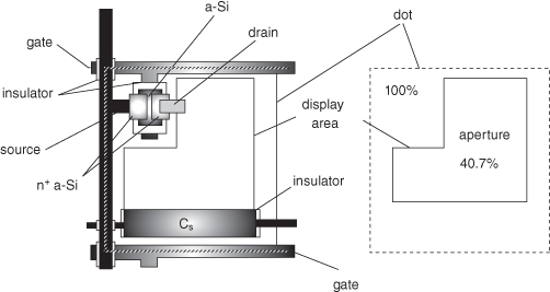
The fundamental cell is shown in an early manifestation in Figure 22.1; each pixel is a dot, and contains an a-Si transistor (denoted by its gate, source, and drain), and a storage capacitor CS. Together with the various insulators, the electronic components take up an area that blocks light passing through, and the ratio of the light transmissive area of pixel to the total area of the pixel is called the aperture ratio of a liquid crystal cell, a ratio to maximize in the design for brighter displays.
Figure 22.1 Early fundamental TFT cell.
Adapted from Yamazaki, T, Kawakami, H., and H. Hori. 1994. Color TFT Liquid Crystal Displays. SEMI, Tokyo.
The active matrix addressing unit mounted on a twisted nematic liquid crystal cell to form a liquid crystal display is shown schematically in Figure 22.2. The liquid crystal layer is bounded by upper and lower transparent ITO plates, which form the electric field; the capacitance of the liquid crystal itself is designated by CLC, the pixel electrode at bottom is connected to the drain of the thin film transistor (TFT) so that when the gate is activated, the image voltages will ...

