5.2 THE CLAMPING CIRCUIT
The clamping circuit essentially consists of an input source, a capacitor of a suitable value and a diode connected in shunt with the output terminals. This clamps the positive peak of the input signal (sinusoidal, in this case) to the zero level. The diode is assumed to be ideal and initially there is no charge on the condenser. vA is the charge built up on the condenser, C. Figure 5.1 shows a basic clamping circuit.
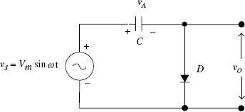
FIGURE 5.1 A negative clamping circuit
As the input rises from 0 to Vm in the first quarter cycle, D conducts [see Figs 5.2(a) and 5.3(a)], C charges to Vm. During this period, vo = 0 if the diode is ideal. ...
Get Pulse and Digital Circuits now with the O’Reilly learning platform.
O’Reilly members experience books, live events, courses curated by job role, and more from O’Reilly and nearly 200 top publishers.

