205Applications
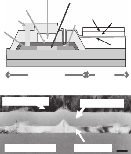
factor. Figure9.8 shows (a) the structure of a poly- Si TFT and
(b) a scanning electron microscope (SEM) image of the layers
of poly- Si, gate insulator, and gate electrode lms after laser
annealing. The hillock formation in the Si layer can be seen [6].
Figure9.9 shows example AFM images from a poly- Si lm
surface (a) after laser crystallization and (b) after Ar- GCIB
irradiation at 20 kV and 1 × 10
16
ions/ cm
2
[7]. By selecting
cluster source materials, irradiation energy, combinations of
different source materials, and glancing- angle irradiation pro-
cessing, surface smoothing by GCIB has effectively eliminated
the hil ...


