Chapter 1. Essential Concepts
An introduction to electronics gives the basics of Ohm’s law; Kirchhoff’s current and voltage laws; current and voltage sources; how resistors, capacitors, and inductors function; and similar topics. A typical curriculum will cover the ideal versions of these topics to clearly convey the basics. Unfortunately, academic simplifications can be misleading. Real-world applications frequently run into problems when ideal concepts fall short. Nothing is ideal.
This chapter takes a brief look at some of the “less than ideal” components seen in real-world applications, how they differ from ideal devices, and where designers need to pay attention to the limitations of nonideal devices. This chapter is about building an awareness of problems that are commonly encountered; the rest of the book develops solutions or strategies to avoid these issues.
To solve any problem, the designer needs to be aware of the problem first. Again, nothing is ideal.
Basic Electronics
There are many textbooks that cover fundamental electronic design from scientific, engineering, and hobbyist perspectives. The focus here is not on basic electronics; rather, it is on the important things that are necessary to design a reliable electronic system. Figures 1-1 and 1-2 serve as a quick checkpoint. If you are reasonably familiar with the topics listed in these figures, you should have the background required to work with the material presented here.
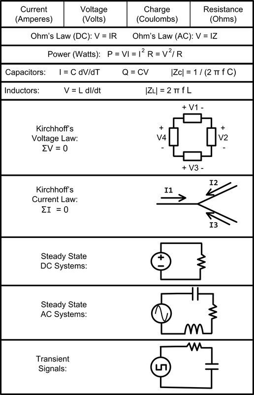
Figure 1-1. Basic concepts, part I
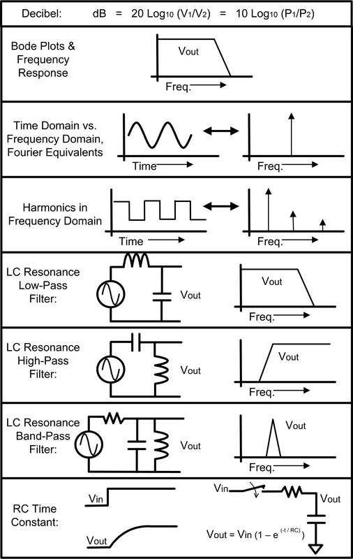
Figure 1-2. Basic concepts, part II
If some items in the figures are unfamiliar to you, there are many reference books, online tutorials, and websites that you can explore. Many of those sources cover the basics.
Ideal Simplifications of Academia
Modern electronic systems are predominantly digital, but most design problems are analog in origin. Noise, signal integrity, power stability, electromagnetic interference (EMI), and connection impedance are common problems. These issues can quickly degrade any electronic system, or render it nonfunctional. Digital systems are more tolerant of these issues, but fully digital devices can be broken by analog limitations.
When explaining electronics, a simplified representation gives a quick idea of how something should work. Such a “first-order” model is useful for simplicity and illustration but frequently leaves out important details. That simple model is often an incomplete model, and many of the “second-order effects” that are omitted can affect device performance significantly.
Becoming aware of a more detailed model helps lay the foundation for better design. The techniques presented here all pay attention to second-order effects and provide methods to deal with them.
Interconnections
As a start, the idea of connecting things together needs a closer look.
As shown in Figure 1-3, a short piece of wire can have significant impedance. A piece of 24 AWG wire, 10 cm long, will have approximately 100 nH of inductance, 10 milliohms of resistance, and capacitive coupling to the environment around it.
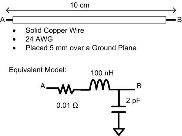
Figure 1-3. Wire impedance
In this example, the wire impedance and capacitance to the outside environment will act as a low-pass filter (LPF) above 300–400 MHz and be sensitive to motion, due to capacitance changing as a function of wire placement relative to ground. Larger wire can reduce resistive losses, and parallel wire connections can reduce inductance some, but the inductance is not easily removed.
A similar 10 cm connection on a printed circuit board (PCB) shows many of the same characteristics. In Figure 1-4, the inductance is about the same as the wire, and the capacitance has increased due to the connection being tightly spaced over a ground plane. For this situation, the PCB trace will start to perform as an LPF around 80–90 MHz due to the increased capacitance. One advantage of the PCB trace over the wire is that the characteristics of the impedance will not change due to the fixed environment that the PCB creates.
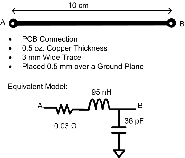
Figure 1-4. PCB connection impedance
The takeaway here is that every connection has impedance, and some coupling to an outside environment.
When connecting things together in Figure 1-5, the impedance of the source, connection, and load plays a part in how much signal loss occurs. Signal loss and distortion get progressively worse with both longer connections and higher frequencies. Designers working under 50 MHz and on a small (10 cm × 10 cm) PCB generally can ignore much of this and survive. High bandwidth, long distances, and connections off the PCB make interconnect issues a significant part of the design problem.
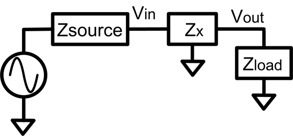
Figure 1-5. Connection impedance
In addition to loading and losses associated with connection impedance, high-frequency signals with a lengthy connection also exhibit transmission line characteristics (Figure 1-6). For the example of the 10 cm connection, current takes about 0.7 ns to transit the wire. Depending on the connection length and the frequency of the signals involved, improperly terminated transmission lines can affect signal integrity.
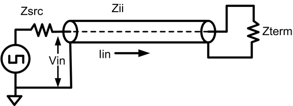
Figure 1-6. Transmission line
Consequently, designers need to consider transmission line issues when the signal wavelength becomes a significant part of the connection distance. For the 10 cm wire example, keeping under 0.1 wavelength on the wire would limit this at a 280 MHz sinusoid. A digital signal has multiple harmonics that need to be included, further limiting the connection’s capability.
The termination impedance, Zterm, should match the characteristic input impedance, Zii, of the line to minimize reflections on the transmission line. Practical applications terminate at both ends of the line (Zsrc and Zterm) to minimize both the initial reflection and any residual reflection that went back to the driven end. The use of impedance matching, striplines, and creating data paths with high signal integrity are topics covered in Chapters 3 and 11 (FDI: Digital, FDI: PCB).
As shown in Figure 1-7, even a solid copper sheet used as a PCB ground plane will exhibit resistance and inductance between locations. A current surge anywhere on a dedicated ground plane will cause that location to have a voltage transition relative to other locations on the ground plane. A surge current into the ground is analogous to a person bouncing on a trampoline. That ground bounce can be kept low by minimizing ground impedance and the magnitude of current surges into the ground.
It is important to recognize the concept that there is not a singular ideal ground, but rather that the voltage of ground can vary, with both the proximity between points and the characteristics of the current dynamics passing through the ground plane.
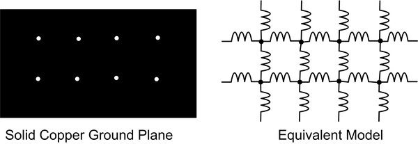
Figure 1-7. Planar PCB connections
Figure 1-8 shows power and ground (P&G) connections exhibiting impedance. The typical electronic device presents switched loads between power and ground, causing the power voltage to drop and the ground to rise. The magnitude of P&G variance is influenced by the connection impedance and the transient rate at which the current changes (di/dt). The transient current can be changed through the load resistance variance and by how much capacitance is present across the load. Proper system design adjusts these variables to give P&G stability that is good enough to maintain proper functionality.
In most situations, P&G bounce can be kept manageable with proper circuit techniques, power bypass filtering, and PCB layout.
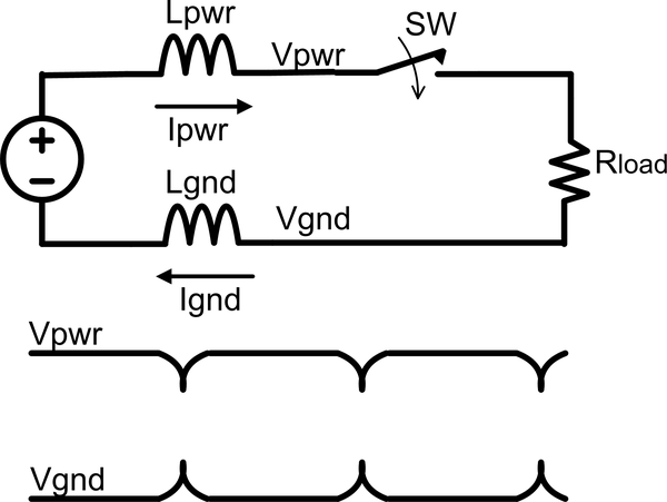
Figure 1-8. Power and ground impedance, ground bounce, and power instability
As shown in Figure 1-9, connections between circuit boards will have signal integrity problems on all connections. Current surges on P&G wires will create voltage variances between the separated boards. That variance makes noise on any ground-referenced signal, relative to the local ground. An external stimulus like EMI or electrostatic discharge (ESD) can further corrupt all signals.
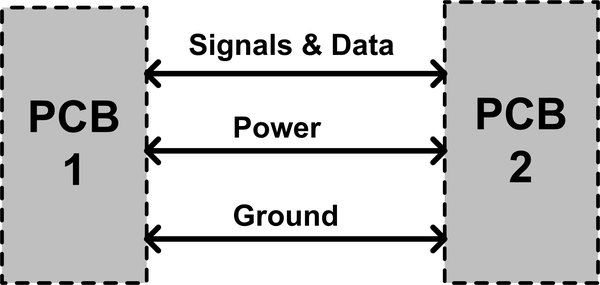
Figure 1-9. Impedance between circuit boards
Special efforts need to be made to “clean up” the noisy raw power coming into the board and create clean power on the PCB. Also, data and signals need to be passed between boards in a manner that is not dependent on local grounds or power supplies. Chapters 3, 4, and 6 deal with these issues (FDI: Power, FDI: EMC & ESD, FDI: Digital).
Distributing a common signal to multiple receivers can result in phase errors between the received signals. Figure 1-10 shows one signal going to five locations. Present in the connection are the distributed connection impedance, path length, and capacitive receiver load. All of these result in five different phases of the original signal. This is a common problem in clock tree distribution, especially with high clock frequencies, multiple destinations, and longer distances.
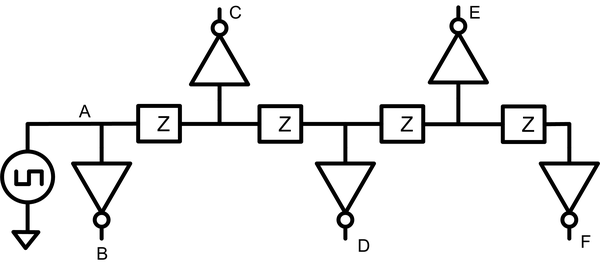
Figure 1-10. Phase errors in digital signals
Frequently, designers don’t consider interconnect issues until problems arise. At that point, an expensive redesign is necessary. When high currents, long connection paths, or high frequencies are involved, they need to be carefully considered in the design.
Basic Components
The evolution of electronics includes a diverse collection of devices, many of which are now obsolete. The emphasis here is on modern systems that will be commercially manufactured in volume. Axial lead devices and other through-hole components are minimized in most high-volume manufactured devices. Consequently, surface mount circuit components are the focus here.
Capacitors
A distributed element model of a surface mount multilayer ceramic capacitor (SMT MLCC) is shown in Figure 1-11. This type of capacitor has multiple interleaved conducting and insulating layers. The actual capacitance is between adjacent plates (C), all plates have a small amount of resistance (R), and the interconnection has inductance (L). A distributed element model can be awkward to work with, and an equivalent model is generally sufficiently accurate.
The equivalent model, also known as a lumped element model, includes elements that model externally observed behavior. This device includes a single Equivalent Series Inductance or ESL (L), a single Equivalent Series Resistance or ESR, a single capacitor, and a leakage resistance (Rleak). The principal capacitor element can vary, primarily as a function of temperature and the voltage across it. The variability is due to the insulating dielectric characteristics used between the plates.
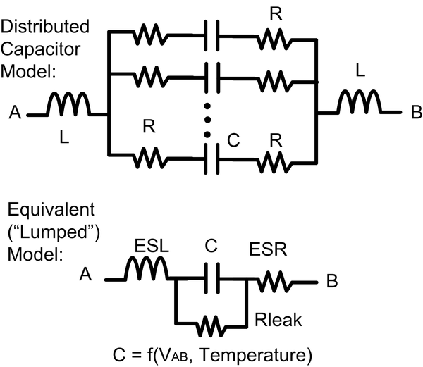
Figure 1-11. Surface mount multilayer ceramic capacitor
Depending upon the application, some elements can be ignored or, in other scenarios, can limit the device’s performance. ESL is important for RF circuit performance and high-frequency power filters but does not affect low-frequency performance. ESL with C creates a self-resonant tuned circuit (Figure 1-12), which limits the high-frequency response of the capacitor.
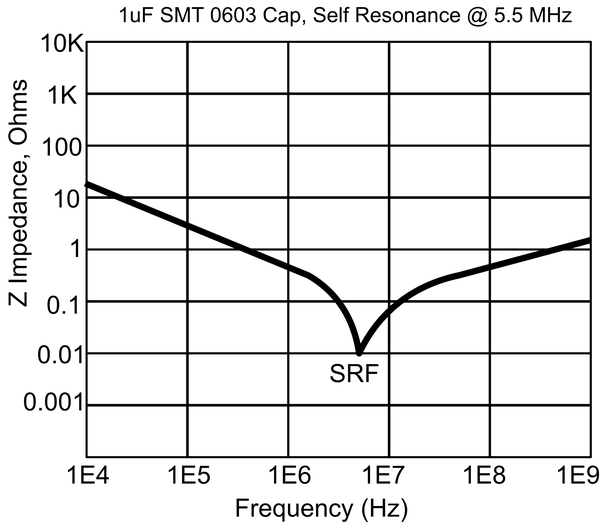
Figure 1-12. Self-resonance of surface mount multilayer ceramic capacitor
Leakage resistance becomes an issue if a capacitor is used to hold a static charge for an extended time. ESR becomes apparent in circuits using high-surge currents through the capacitor. The SMT MLCC makes up the majority of PCB capacitors due to excellent reliability, low cost, and the wide selection of options available.
Modern capacitors make trade-offs in:
Capacitance per unit volume
Maximum applied voltage (breakdown voltage)
Min/max operating temperatures
Temperature variation from nominal value
Applied voltage variation from nominal value
Aging variation from nominal value
Nominal value accuracy
Total overall life
These parameters interact with each other. If the manufacturer changes one parameter, the change can affect another parameter. For example, creating a higher breakdown voltage implies a larger body size for the same value of capacitance.
SMT MLCCs have different dielectrics, which leads to different performance parameters. Looking at the more common devices, some brief comments are useful to better understand the differences.
C0G and NP0 are known as Class 1 capacitors, which are designed for minimal thermal variance and minimal change from voltage bias. Class 1 devices sacrifice capacitance per unit volume to achieve higher accuracy and stability. For a given body size, the total capacitance is limited. These devices are useful for tuned circuits and other applications where accuracy and stability are needed.
X5R, X7R, Y5V, and others are known as Class 2 capacitors (Table 1-1). Their design sacrifices voltage bias accuracy and thermal stability to achieve more capacitance within a given volume. The notation used for these devices is a little confusing but actually simple to decode. The three characters decode to a minimum temperature, maximum temperature, and value variance over temperature. An X7R capacitor is designed for use from −55°C to 125°C and will have +/−15% variance over temperature. The Y5V capacitor is designed for use from −30°C to 85°C and will have a value ranging from +22% to −82%. Picking the proper capacitor dielectric can significantly affect accuracy.
| Low temperature (°C) | High temperature (°C) | Temperature variance |
|---|---|---|
| X = −55 | 4 = 65 | P = +/−10% |
| Y = −30 | 5 = 85 | R = +/−15% |
| Z = 10 | 6 = 105 | S = +/−22% |
| 7 = 125 | T = +22%, −33% | |
| 8 = 150 | U = +22%, −56% | |
| 9 = 200 | V = +22%, −82% |
Class 2 devices also exhibit DC bias effect, also known as the DC voltage characteristic, which consists of changes to the capacitance value as a function of the static DC voltage across the device. Generally, the value of the capacitance decreases as the bias voltage increases. This can be significant, with as much as 60% of the capacitance value changing depending on the specifics of the device.
Devices with a higher breakdown voltage tend to have less DC bias effect for the same voltage change. This can be useful if a designer needs to reduce this effect. If a specific capacitor needs high accuracy, a Class 1 capacitor may be required.
Entire books have been dedicated to capacitors. A closer look at the limitations of the SMT MLCC is warranted because it is the predominant capacitor used in modern designs.
Several other capacitors are frequently used in modern designs. The aluminum electrolytic capacitor (AEC) is widely used in DC power supply filters and other applications where large amounts of capacitance in a small package, coupled with low cost, are needed. All AECs suffer from poor high-frequency response due to high ESL, so AECs are not suitable for RF situations. High-frequency response of the AEC can be supplemented by parallel SMT MLCC devices if needed. The AEC also has a limited life, fussy temperature restrictions, and significant ESR. Check device specifications for aging information and lifetime versus temperature data. Most AEC devices have performance and lifetime parameters that are unique to a specific manufacturer and product line.
Both tantalum and aluminum-polymer capacitors are available in high-reliability and long-life variants. Component selection here needs to be done on a case-by-case basis because these devices also have short life variants as well.
Following are important things to look for in a capacitor:
Nominal component value and fabrication tolerance
Breakdown voltage
Package size
Dielectric type, temperature range, and variance over temperature
DC bias effect and device variation due to bias voltage
ESL characteristics and self-resonant frequency (SRF)
for high-frequency applicationsESR characteristics where series resistance can affect performance
Resistors
A typical resistor model is shown in Figure 1-13. In addition to the ideal resistance (R), some additional elements need consideration. These are ESL, Equivalent Parallel Capacitance (EPC), and internally generated noise (Vn) created by the resistance itself.
Ideally, a resistance has flat impedance over frequency. Because of EPC and ESL, the impedance may not be flat at high frequencies. For DC bias applications, the ESL and EPC can be ignored. Multiwatt resistors are commonly fabricated with wire-wound methods and have significant ESL and EPC components.

Figure 1-13. High-frequency resistor model
Most modern surface mount resistors are some type of film resistor: thick film, thin film, and metal film are common descriptions of devices available. Multiple vendors have found many different approaches to making resistors. Generally, metal film resistors exhibit lower noise than carbon and thick film devices, but check specific vendors for noise data.
Thermal noise, also known as Johnson-Nyquist noise, is created by the thermal agitation of electrons in a resistive material. For most large-signal applications, this noise is not a significant issue. It becomes important in RF frontends, communication channels, and low-amplitude scenarios, where signals are in the nanovolts.
Gigaohm resistors are available from manufacturers, but special considerations have to be made to use them. Dust and humidity (Figure 1-14) in the environment can have a lower impedance path than the resistor. As a general rule, anything over 100 K ohms needs special environmental attention to avoid alternative current paths around the resistor.
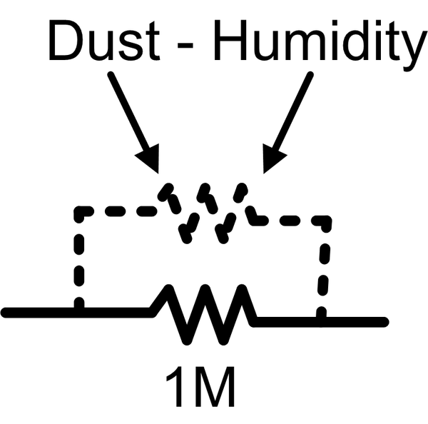
Figure 1-14. Environmental sensitivity of high-impedance resistors
Thankfully, most modern designs don’t need high-value resistors, because the analog circuits that used them in the past have been replaced with more reliable digital methods.
The following are important things to look for in a resistor:
Nominal component value and fabrication tolerance
Material composition; film resistors are preferred, older carbon-based resistors should be avoided
Power rating
Min–max temperature range
Maximum voltage rating for high-voltage applications
Thermal variance, sometimes specified as temperature coefficient of resistance
ESL for high-frequency situations
Thermal noise, carbon contact noise
Stability, repeatability, and aging data
Inductors
A high-frequency model of an inductor is shown in Figure 1-15. Some EPC exists, which limits the useful frequency range. With EPC and L in parallel, the device will resonate as a tank circuit and look like an open circuit at the SRF. Below the SRF, the device functions as an inductor; above the SRF, the device performs like a capacitor.
The ESR defines the quality factor (Q) of the inductor when used as part of a filter. When used in a switching power converter, the ESR will limit power efficiency.
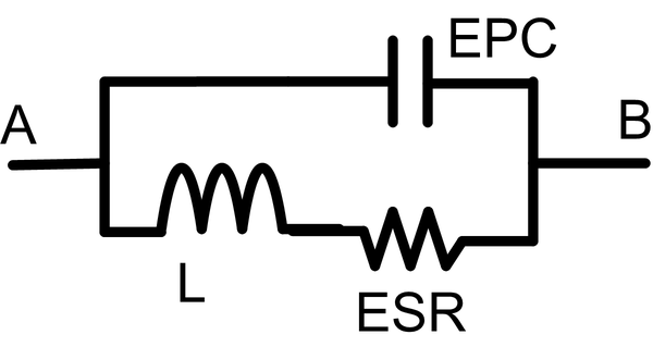
Figure 1-15. High-frequency inductor model
Inductors are commonly used in power conversion, RF signal processing, and EMI limiting. Inductors are used in switched-mode power conversion, in both AC/DC and DC/DC converters. Inductor priorities for power conversion are maximum current, saturation current, thermal range, and resistive losses. Switching converters have high current transients, and suitable devices are wire-wound on a magnetic core, with high current capability and low resistive losses (FDI: Power).
Inductors in RF signal processing are used in tuned circuits and need consistent accuracy for reproducible frequency response. Priorities are a high quality factor, component tolerance/accuracy, and ensuring that the SRF does not affect the signals being processed. Lower currents are used in signal processing inductors, and many components exist in surface mount variants.
Inductors used for EMI limiting are commonly known as chokes. Their purpose is to pass DC current while reducing transient currents in the connection. High-current chokes are commonly implemented with a wire-wound power inductor. Low-current chokes can be implemented with smaller surface mount inductors (FDI: EMC & ESD).
Following are important things to consider in an inductor:
Whether the component value and tolerance will meet the design’s required accuracy
SRF and whether it affects the signals of interest
Current rating, peak and average
Temperature range
Core material and saturation current
DC resistance and device Q
Whether it is shielded or unshielded
Voltage Sources and Batteries
The ideal voltage source doesn’t exist. An infinite source of current at a fixed voltage is an academic concept. Practical implementations of a voltage source can be the output of a voltage regulator, a battery, or another generation source. Invariably, these all have limitations.
Any detailed voltage source model (Figure 1-16) includes source resistance (Rsrc), a noise component (Vnoise), and the voltage source being a dependent function of the output current (Iload). The goal of a voltage source design is to minimize the Rsrc, the Vnoise, and the dependency on Iload.
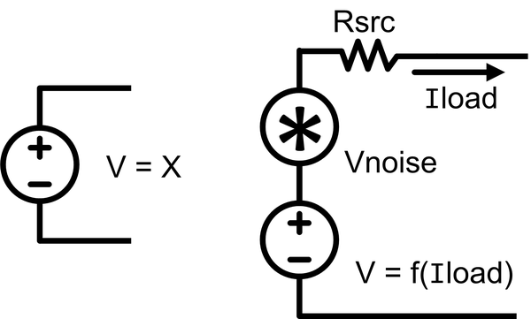
Figure 1-16. Voltage sources, ideal (left) versus real (right)
Batteries have a limited capacity, so voltage variation over discharge has to be added to the model. Also, batteries have current limitations around charging and discharging, reduced performance with age, and a myriad of special considerations depending on the particular battery type. Chapter 5 is devoted to the design, care, and feeding of battery supplies (FDI: Battery).
The characteristics of the Vnoise signal will be highly dependent upon the methods used to create the voltage source. Linear power supplies and regulators that have been carefully optimized for noise are available when low-noise power is needed. Batteries are very low noise, but they are not perfect, and they can generate electrochemical voltage noise dependent on charge state, or the battery charger can superimpose noise onto the power.
Switching power supplies will achieve high efficiency while generating commutation noise associated with the voltage regulation function. Digital electronics don’t need ultra-low-noise power, but any chip designed into a system needs to be investigated for its “noise on the power” limitations.
Current Sources
Similar to ideal voltage source, an ideal current source doesn’t exist. A number of circuit designs come close but have restrictions and limitations on impedance and voltage range.
A practical current source (Figure 1-17) includes some source resistance (Rsrc), a noise component (Inoise), and an output current that is a dependent function of the output voltage (Vout).

Figure 1-17. Current sources, ideal (left) versus real (right)
Most current sources are limited in voltage range to maintain appropriate, fixed-current behavior. Discrete current sources are not commonly used in board-level system on a chip (SoC) design, but they are an important building block within analog and mixed-signal integrated circuit (IC) design. Readers interested in this topic can research “Cascode current sources” for further information.
Switches and Relays
Mechanical switches and relays can be problematic, especially if they are used as control inputs on a logic port. Both exhibit similar problems due to their mechanical implementations.
For instance, mechanical switches and relays exhibit contact bounce (Figure 1-18), where the process of opening and shutting contacts creates multiple brief open/shut states. If they are used as digital logic inputs, opening and closing contacts are seen as an erratic string of data states due to imprecise mechanical contacts. Using a switch on a logic port requires software polling the port multiple times and determining state change after remaining stable for 50–100 ms.
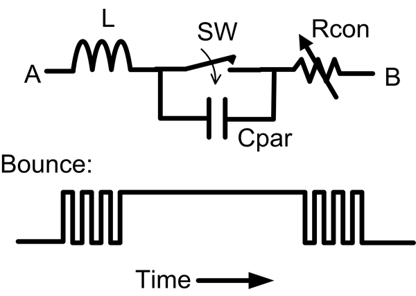
Figure 1-18. Switches and relays with contact bounce
In addition to contact bounce, switches have inductance (L) that adds impedance to a closed switch. Parasitic capacitance (Cpar) allows high-frequency signals to pass through an open switch. Also, contacts have highly variable resistance (Rcon) and can change with every switch cycle. This variability gets worse with age as contacts become dirty or damaged.
Operational Amplifiers
The ideal operational amplifier (op-amp) claims to have infinite gain, infinite bandwidth, infinite voltage range, infinite current output, zero input current, zero noise, zero offset voltage, and, best of all, no need for a power supply. As a math model, it’s an interesting idea, but reality is something else.
The real op-amp (Figure 1-19) has limitations that affect performance. First, the device requires power and ground (Vpower, Vgnd), and the output (Vout) can be sensitive to noise present (NP, NG) on these connections. The output has impedance (Rout), and the output voltage (Vout) is restricted by the power supply voltage. The gain is not infinite; rather, an open loop gain of 80 dB is typical.
The gain response over frequency will have both bandwidth limitations and an additive phase response. Also, the output response speed is limited by a maximum slew rate at which the device can respond. Since an op-amp is designed to function within a closed feedback system, the high-frequency gain of the device must be internally limited to keep it stable within a feedback configuration. Due to this frequency compensation, op-amps may not be the best devices to use in high-frequency designs.
Input capacitance (Cinp) creates loading that can affect high-frequency performance. Op-amps designed with bipolar transistors will have input bias current (Ibias). The input transistors used within the op-amp will not be perfectly matched and will create an equivalent input offset voltage (Voff) that is typically 1–10 mV depending on the specific device. That offset voltage becomes a problem when dealing with small signals or high-gain closed loop configurations. The internal circuitry will create noise, which is modeled as an input referred noise (IRN) source.
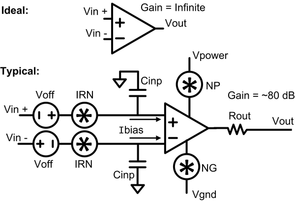
Figure 1-19. Ideal versus typical op-amp
Many of these limitations are not a problem when working with larger signals, but pushing for high gain and high bandwidth or using sub-mV signals will show performance limitations. Performance specifics will depend on the op-amp selected, and many offerings are commercially available.
Voltage Comparators
A voltage comparator has many things in common with the op-amp model. The comparator (Figure 1-20) also has sensitivity to power and ground noise (NP, NG), input loading capacitance (Cinp), IRN, and input offset (Voff), similar to an op-amp. Since the typical application is against a fixed reference voltage (Vin −), a simple one-sided model will suffice.
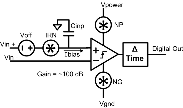
Figure 1-20. Typical comparator
The difference between an op-amp and a comparator centers on the fact that an op-amp is designed to function within an analog feedback loop and a comparator is not. Comparator gain is often higher (~100 dB), no internal frequency compensation is used, and the output is digital.
A variable time response is part of a comparator model since input/output time can be dependent on the input signal amplitude. Small signals with a minimal crossover voltage are slower to propagate through the circuit than a larger voltage transition.
Nonideal Digital Devices
Digital devices are generally more resilient to noise than analog signals. However, even digital systems have nonideal problems and limitations.
Figure 1-21 shows communication between two digital devices. In modern designs, discrete gates are uncommon, but this illustrates communication between any two digital devices, such as field-programmable gate arrays (FPGAs), microcontrollers, or other devices that share a common P&G.
As illustrated, the P&G between devices includes connections with distributed inductance. Depending on what else is connected to the P&G network, currents drawn from or injected into the network can cause the connection to reactively dip or rise. As well, the magnitude of that “bounce” can be different at various locations on the network.
In Figure 1-21, the P&G network at one location (VPWR1, VGND1) has different characteristics than at another location (VPWR2, VGND2). How much of this bounce is tolerable depends on the transistor technology used in the digital gates, but keeping the P&G stable has to be a priority.
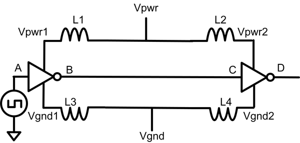
Figure 1-21. Impedance-created voltage differences across power and ground
Generally, CMOS semiconductors are designed with transistor threshold voltages that are about one-third of the power supply voltage and can tolerate P&G instability of 20% of the nominal power before digital devices start to generate false states. Any commercial product will specify acceptable voltage ranges for both high and low logic states. That specification is a quick guideline to how much P&G noise is tolerable.
As shown in Figure 1-22, a clean two-state signal at A can be corrupted by unstable P&G (VPWR1, VGND1) at its output (B), which is then further disturbed by the variation in P&G (VPWR2, VGND2) at the receiving end (C), leaving an output (D) that no longer represents the original signal.
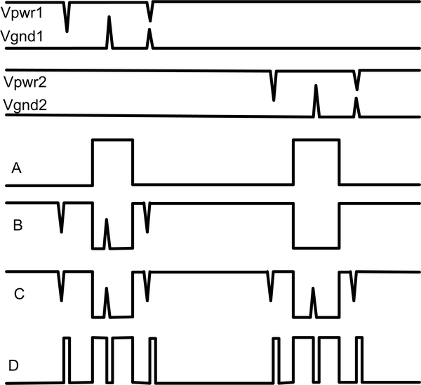
Figure 1-22. Digital sensitivity to power and ground noise
False state generation is just one of many problems seen in digital systems. Consider the clocked system shown in Figure 1-23, with two devices communicating at the same frequency but using uncorrelated clocks. Although the clocks are the same frequency, there is no fixed-phase relationship between devices. As phase changes, the data–clock relationship periodically violates setup and hold times, and data errors occur. Chapter 3 (FDI: Digital) covers techniques to deal with reliable unsynchronized data transfer.
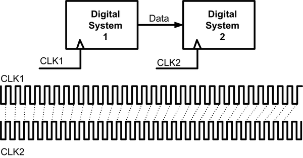
Figure 1-23. Unsynchronized digital system with variable phase
Asynchronous logic should be avoided due to unpredictable outputs and digital glitches. Although Figure 1-24 is a bit contrived, the Boolean analysis says the output (C) should never assert. Reality shows that the propagation delay of the inverter affects output. This illustrates the motivation for synchronous logic where data resynchronization to a clock is used to avoid glitches.
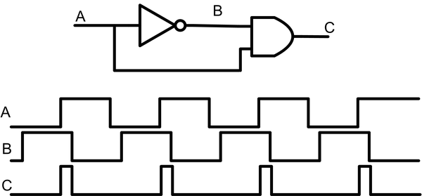
Figure 1-24. Race conditions in asynchronous logic
In addition to problems created by timing relationships, digital functionality can suffer due to the analog characteristics of digital signals. Several factors can contribute to this: higher data rates, resistance of the transmission path, or a transmission path that is loaded with capacitance.
A simple driver and receiver pair is shown in Figure 1-25. The middle diagram in the figure shows the interconnect impedance with resistance of the PCB (Rpcb), inductance (Lpcb), and capacitance (Cpcb). The bottom diagram in the figure includes an equivalent model for the output driver and receiver. For CMOS logic, the output driver can be modeled as a pair of switches and a resistor. Rout, depending on the transistors used, will typically be 10 Ω to 80 Ω. In addition, the receiver input behaves as a capacitance for most situations. This input capacitance is due to large, high-current ESD protection circuits, and 2 pF to 10 pF is common for each logic gate. Ignoring interconnect inductance, this model shows that an RC low-pass filter is present in every digital interconnect.
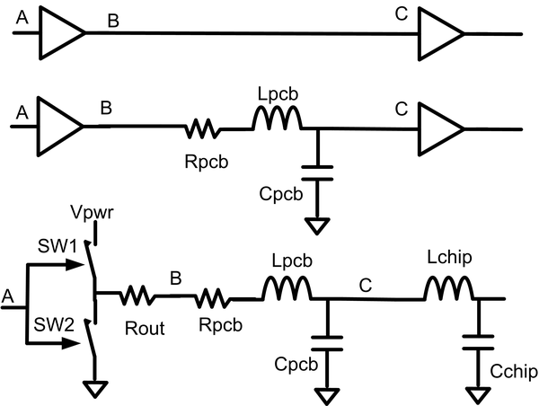
Figure 1-25. RC loading in digital logic interconnects
With this more detailed model, the frequency limitations of logic are apparent. Figure 1-26 illustrates the limitations created by the RC circuits due to the output driver resistance and attached capacitance. On the left, at lower frequencies, enough time is available for the transient behavior to settle out before the next transition. On the right, as time is reduced between transitions, the device has insufficient time to settle out. The RC time constant of the system remains the same, but no well-defined logic states are achieved.

Figure 1-26. RC loading and signal degeneration
The system fails when Vhigh or Vlow limits are violated, or when setup and hold times on flip-flops are not met. Ground referenced logic frequently fails when used for high-frequency communication. Differential signals are commonly used at high data rates to minimize this limitation (FDI: Digital).
Signal Integrity
Undesired effects can be created by a circuit in addition to its normal functionality. Many electronic systems create unwanted electronic noise by creating signals that radiate externally. Also, one part of a system can create noise that interferes with the proper functionality of a different part of the same system. In some cases, a poorly designed system can be sensitive to externally created electromagnetic interference. Signal integrity, radio frequency interference (RFI), EMI, electromagnetic compatibility (EMC), electronic noise, RF immunity, electromagnetic shielding, radiated emissions, crosstalk, and others are all related topics in this area.
Using the 10 cm connection discussed earlier, Figure 1-27 creates radiated emissions with an ideal quarter-wavelength antenna at about 700 MHz. For this example, a 100 MHz clock would have its seventh harmonic have an optimal antenna, making the connection a radio transmitter. All frequencies would radiate from that connection, albeit with varying amounts of efficiency.
Radiated emissions are especially problematic from computers and from any device with large amounts of high-frequency digital circuitry. The Federal Communications Commission (FCC) and other worldwide regulatory bodies restrict the EMI that any device is allowed to produce to minimize interactive problems between electronic devices (FDI: EMC & ESD).

Figure 1-27. Radiated emissions
As illustrated in Figure 1-28, as well as radiating EMI to the outside world, devices can be internally sensitive to unintended communication between circuits, commonly called crosstalk. This noise coupling can be capacitive or magnetic and often takes both paths. This illustrates a common problem with digital signals, especially high-frequency signals, as these can be coupled to an unconnected circuit path (FDI: Digital, FDI: EMC & ESD, FDI: PCB).
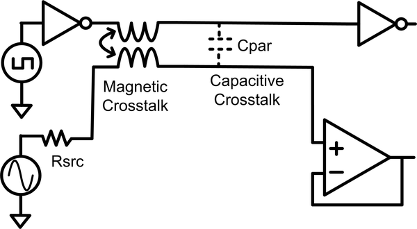
Figure 1-28. Sensitivity to external signals
Summary and Conclusions
The important points of this chapter are as follows:
Academic simplifications often omit important details for the sake of clarity.
All connections have impedance, which can cause voltage variance across P&G.
Phase errors between receivers can exist even when driven by a common signal.
Capacitors have ESL, ESR, self-resonance, leakage, and voltage variance issues.
Resistors have issues with ESL, EPC, and thermally generated noise.
High-impedance resistors are susceptible to error due to environmental issues.
Inductors have ESR, EPC, and self-resonance issues.
Voltage and current sources can have both impedance and noise components.
Switches have contact bounce, inductance, and variable contact resistance.
Op-amps have limitations including input/output voltage range, bandwidth, offset, output current, additive noise, and others.
Comparators have limitations in voltage range, input offset, response time, and others.
Power–ground instability can corrupt logic.
Asynchronous logic can create unpredictable behavior.
Ground-based logic can be limited by RC loading that degenerates signal rise time and amplitude.
Digital devices often create radiated emissions.
Signals in one circuit can couple to another circuit without a direct connection.
The intent of this chapter is to build awareness of the limitations and nonideal nature of electronics. Many engineers build awareness due to device failures from many of the issues described here. Learning from experience is invaluable, but failure analysis is not the most efficient use of time or effort.
Moving forward, the techniques presented in this book address these limitations while developing design solutions proven to work in real-world applications.
Further Reading
“Capacitor Guide – Dielectric Materials,” EETech Media, LLC, www.capacitorguide.com/dielectric-materials.
“Understanding Ceramic Capacitors: types – MLCC, C0G, X7R, Y5V, NP0, etc.,” Electronics Notes, https://www.electronics-notes.com/articles/electronic_components/capacitors/ceramic-dielectric-types-c0g-x7r-z5u-y5v.php.
“Here’s What Makes MLCC Dielectrics Different,” Kemet Corporation, https://ec.kemet.com/blog/mlcc-dielectric-differences.
“Types of Capacitors: An Essential Overview,” Electronics Notes, https://www.electronics-notes.com/articles/electronic_components/capacitors/capacitor-types.php.
“High-Reliability Capacitors: When the Mission Just Can’t Fail,” Kemet Corporation, https://www.aerodefensetech.com/component/content/article/adt/features/articles/27962.
C.K. Boggs, A.D. Doak, and F.L. Walls, “Measurement of Voltage Noise in Chemical Batteries,” Proceedings of the 1995 IEEE International Frequency Control Symposium (49th Annual Symposium), May 31–June 2, 1995.
Analysis and Design of Analog Integrated Circuits, 5th Edition, by Paul R. Gray, Paul J. Hurst, Stephen H. Lewis, and Robert G. Meyer, 2009, ISBN 978-0-470-24599-6, John Wiley & Sons.
Get Applied Embedded Electronics now with the O’Reilly learning platform.
O’Reilly members experience books, live events, courses curated by job role, and more from O’Reilly and nearly 200 top publishers.

