7.8 Electrical Structures
The most widely used structure is a p–i–n diode, which is basically a two-terminal device. The structure gave way to three terminal structures which are either p–i–n devices or a bipolar mode field effect transistors (BMFETs). The most recent configuration giving encouraging results is a metal–oxide–silicon (MOS) capacitor. In the following, we discuss the features of the structures giving the schematic diagrams. The discussion is mostly based on the review by Reed and Png [15].
7.8.1 p–i–n Structures
The waveguide intensity modulator using free-carrier absorption was first fabricated by Treyz et al. 16 to work in the 1.3–1.55 µm range. The schematic diagram of the structure used is shown in Figure 7.5.
Figure 7.5 Schematic diagram of the p–i–n structure used by Treyz et al. (EDL (1991) [16]).
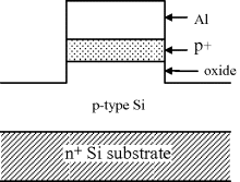
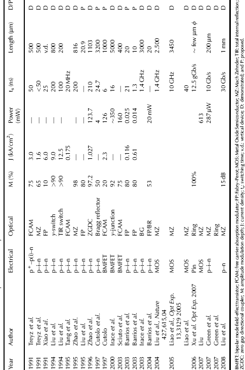
The intrinsic region is a p− region having a doping concentration < 5 × 1015 cm−3, while the p+ region has a doping concentration > 5 × 1019 cm−3. By applying a forward bias to the device, free carriers are injected into the p-type Si-guiding layer. The characteristic of the modulator is given in Table 7.1. The switching time corresponds to change from 90% to 10%.
Table 7.1 All-silicon electro-optic modulators reported in the literature.
The waveguide possesses a ...
Get Silicon Photonics: Fundamentals and Devices now with the O’Reilly learning platform.
O’Reilly members experience books, live events, courses curated by job role, and more from O’Reilly and nearly 200 top publishers.

