CHAPTER FIVE
Design Example of Programmable Timer
Chapter 3 explained the basic concept of Verilog, and Chapter 4 showed some common known coding methods that are used in synthesis. Chapter 5 shows an example of how a real-life practical design can be achieved, beginning from design specification, architectural definition, coding, and verification.
The example discussed in Chapter 5 is a design of a programmable timer. Timers are common design modules in almost all types of system. The design of the programmable timer begins with a design specification for its features and capabilities.
5.1 PROGRAMMABLE TIMER DESIGN SPECIFICATION
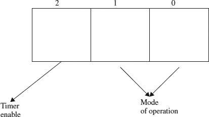
The programmable timer is an eight-bit timer that allows three different modes, a one-shot timer, a pulse generator, and a 50% duty cycle waveform generator. For each mode, a certain value can be loaded into the timer before the timer begins clocking. The timer can determine which mode to operate in by using an internal register. This internal register is referred to as “control word register.” The control word register is a three-bit register with the MSB bit representing “timer enable” and bit 1 and bit 0 represents the mode of operation.
Referring to Figure 5.1:

FIGURE 5.1. Diagram showing bits of control word register.
- Timer enable—this bit if set to a “1” would enable the timer.
- Mode of operation:
- Mode “00”—one-shot timer. In this mode, the timer ...
Get Verilog Coding for Logic Synthesis now with the O’Reilly learning platform.
O’Reilly members experience books, live events, courses curated by job role, and more from O’Reilly and nearly 200 top publishers.

