May 2003
Intermediate to advanced
192 pages
3h 50m
English
A simplified block diagram of a PLL is shown in Figure C.1. The reference clock, REFclk, is the input clock into the ASIC. The PLL tracks the reference clock and adjusts the phase of its output, PLLout, such that REFclk and the feedback clock, FBclk, are in phase.
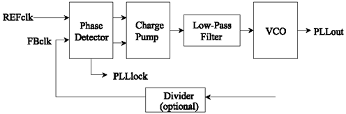
The phase detector compares the phase difference between the rising edge of REFclk and the rising edge of FBclk. When the two are not aligned, the phase-detector output changes to increase or decrease the voltage level on the output on the charge pump.
The charge pump and low-pass filter convert the digital output of the phase detector ...
Read now
Unlock full access


 O’Reilly covers everything we've got, with content to help us build a world-class technology community, upgrade the capabilities and competencies of our teams, and improve overall team performance as well as their engagement.I wanted to learn C and C++, but it didn't click for me until I picked up an O'Reilly book. When I went on the O’Reilly platform, I was astonished to find all the books there, plus live events and sandboxes so you could play around with the technology.I’ve been on the O’Reilly platform for more than eight years. I use a couple of learning platforms, but I'm on O'Reilly more than anybody else. When you're there, you start learning. I'm never disappointed.I'm always learning. So when I got on to O'Reilly, I was like a kid in a candy store. There are playlists. There are answers. There's on-demand training. It's worth its weight in gold, in terms of what it allows me to do.