6.2 ARCHITECTURE OF THE CHS2×4
The architecture of Algotronix’s configurable array logic (CAL) technology [Algo91] is particularly suited to the building of arrays of chips to form a single computing surface [Gray89]. The CHS2×4 and its associated software have been designed and built to explore this aspect of FPGA usage.
The CHS2×4 contains up to 9 CAL1024 chips and 2M bytes of static RAM. Two boards can be connected together to form a system with a 4 × 4 array of CAL chips for computation and up to 4M bytes of static RAM. The CHS2×4 board is supported by the configurable logic software (CLS) software suite, including a graphical editor and an on-line debugger, and a library of interface routines that can be called from the user’s C programs.
6.2.1 Hardware Architecture
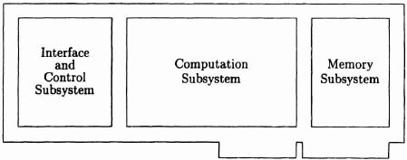
Architecturally the CHS2×4 system consists of three hardware subsystems (see Figure 6–1). These are:
- PC interface and control subsystem.
- computation subsystem.
- memory subsystem.
The bus architecture, Figure 6–2 allows the memory subsystem and CAL configuration memory of the computation subsystem to be read and written from the host processor. Configuration memory and the memory subsystem share an address space local to the board. In addition, the computation array may execute memory operations, using the counter as an address register, synchronized to the host clock.

Figure 6–1. CHS2×4 board. Figure courtesy ...
Get Field-Programmable Gate Arrays: Reconfigurable Logic for Rapid Prototyping and Implementation of Digital Systems now with the O’Reilly learning platform.
O’Reilly members experience books, live events, courses curated by job role, and more from O’Reilly and nearly 200 top publishers.

