96
D2
D5
D6
D7
A
Logic analyser
B C D
Clock
\Z\
K
HLT
0 R/W INT
NMI
CPU
ROM
K
il/
1
—\[
sh—Λ
RAM
K
^L^C
16
System I/O
JTL
"L_T
_n_
1_T
16
L
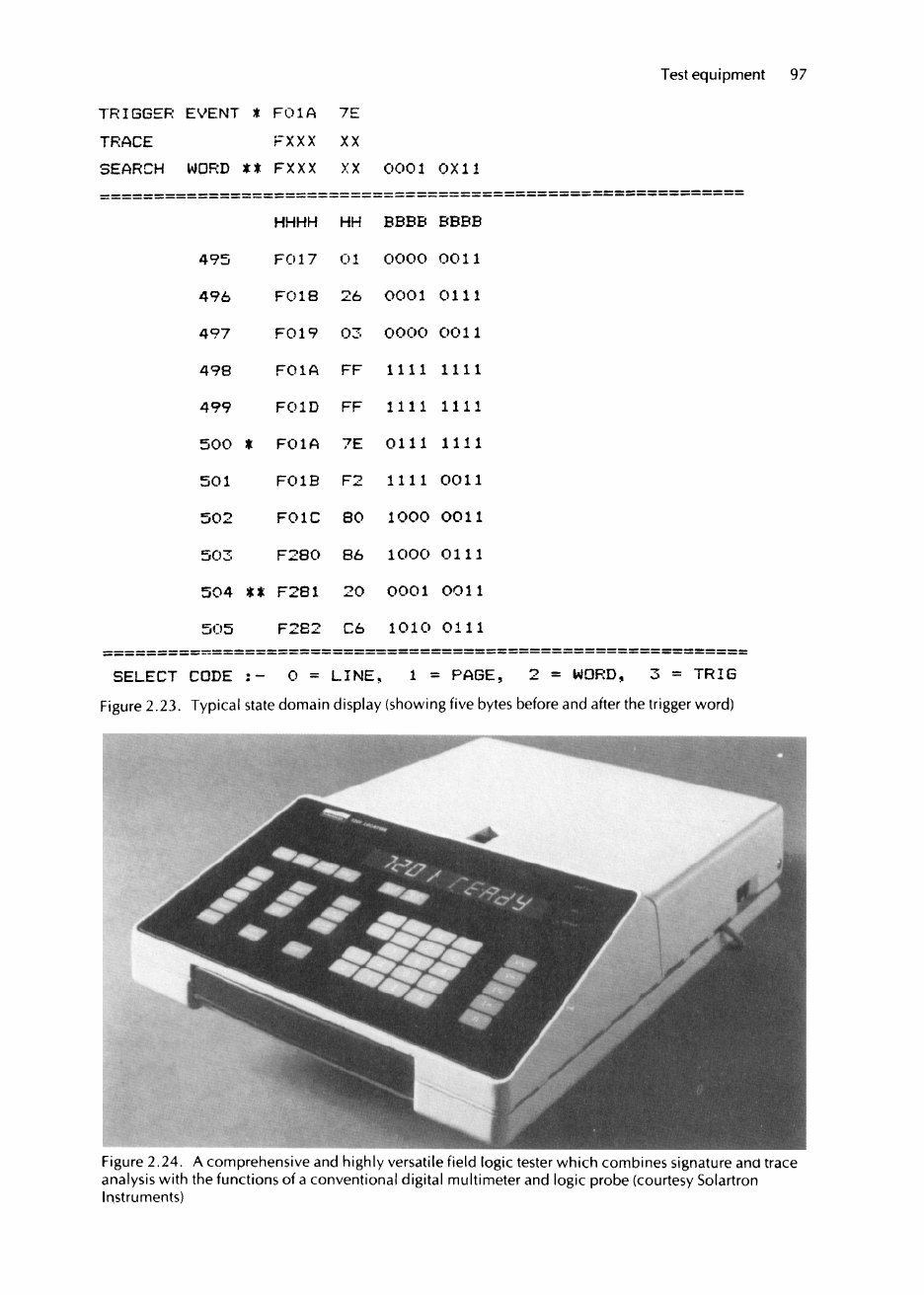
Figure
2.21.
Connection of a logic analyser
to a microcomputer
Figure 2.22. Typical time domain display
(the cursor is positioned over the data word
10101011)